Wafer flow sheet surface flatness detection device capable of avoiding false flaws

A surface flatness and detection device technology, which is applied in semiconductor/solid-state device testing/measurement, electrical components, semiconductor/solid-state device manufacturing, etc., can solve problems such as increasing processing costs, reducing production efficiency, and inaccurate data, so as to avoid Secondary maintenance, reduce processing costs, scan comprehensive effect

Active Publication Date: 2019-07-16
SHENZHEN SMARTMORE TECH CO LTD +1
View PDF7 Cites 4 Cited by
  • Summary
  • Abstract
  • Description
  • Claims
  • Application Information

AI Technical Summary

Problems solved by technology

[0004] The main purpose of the present invention is to overcome the deficiencies of the prior art and provide a device for detecting the surface flatness of wafer tape-outs that avoids false defects, so as to solve the problem of dust falling or tiny parts falling frequently during wafer processing. On the wafer, the data is inaccurate when the equipment scans the wafer, and the qualified wafer is judged as a defective product, resulting in a secondary inspection of the qualified product, which increases the processing cost and reduces the production efficiency.

Method used


Image

  • Wafer flow sheet surface flatness detection device capable of avoiding false flaws
  • Wafer flow sheet surface flatness detection device capable of avoiding false flaws
  • Wafer flow sheet surface flatness detection device capable of avoiding false flaws

Examples


Embodiment Construction

[0026] The following will clearly and completely describe the technical solutions in the embodiments of the present invention with reference to the accompanying drawings in the embodiments of the present invention. Obviously, the described embodiments are only some, not all, embodiments of the present invention. Based on the embodiments of the present invention, all other embodiments obtained by persons of ordinary skill in the art without making creative efforts belong to the protection scope of the present invention.

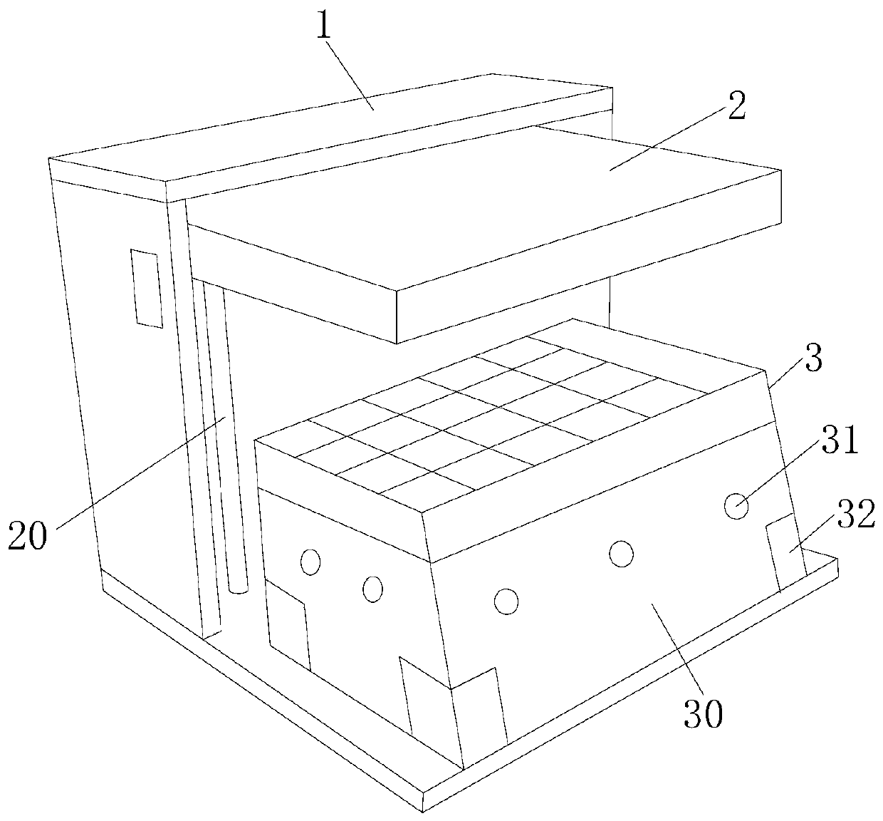
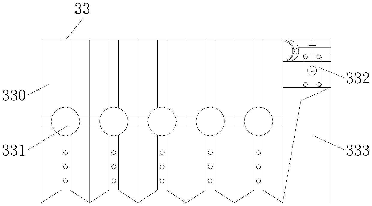
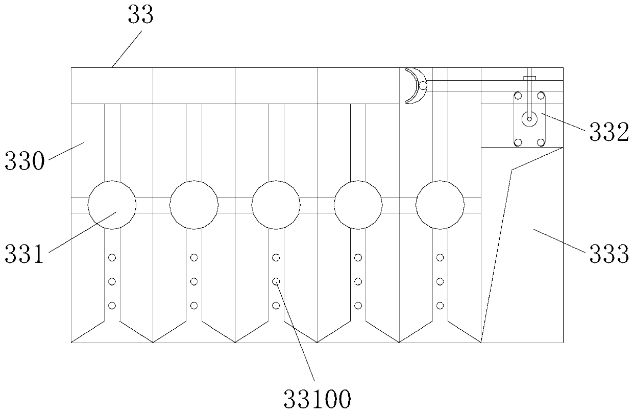
[0027] see Figure 1-9 , the present invention provides a technical scheme of a wafer surface flatness detection device that avoids false defects: its structure includes a test frame 1, a scanning board 2, and a delivery table 3, and the test frame 1 is connected to the scanning board 2 by rails. The scanning board 2 is threadedly connected with a threaded rod 20, the threaded rod 20 is installed on the test frame 1, the scanning board 2 can be lifted, and the...


PUM


Abstract

The invention discloses a wafer flow sheet surface flatness detection device capable of avoiding false flaws. The wafer flow sheet surface flatness detection device structurally comprises a test frame, a scanning plate and a conveying table; the test frame is in track connection with the scanning plate; the scanning plate is in threaded connection with a threaded rod, and the threaded rod is arranged on the test frame; the test frame is locked with the conveying table; the conveying table is composed of a surrounding frame, a lock hole, a lock plate and an internal device; the surrounding frame is provided with the lock hole and the lock plate; the internal device is arranged on the surrounding frame; when the wafer is in assembly line processing and passes through a detection device, thescanning plate is adopted for scanning detection; if the products are qualified products, the qualified products are continuously conveyed to the next procedure on the conveying table; and if defective products are detected, the internal device operates, and secondary scanning detection is carried out by the internal scanning device; the side scanning of the internal scanning device can judge whether the flaws are pseudo flaws or not more accurately, so that secondary overhauling of qualified products is avoided, the processing cost is lowered, and the production efficiency is improved.

Description

technical field [0001] The invention relates to the field of semiconductors, in particular to a device for detecting the surface flatness of wafer tape-outs which avoids false defects. Background technique [0002] The detection of the flatness of the wafer surface is for the needs of lithography and for the performance considerations of integrated circuits; tape-out refers to the manufacture of chips through a series of process steps like an assembly line; in the field of integrated circuit design, "flow-out" refers to It is "trial production", that is to say, after the circuit is designed, a few dozens of pieces are produced for testing. If the test passes, mass production will start like this. [0003] In the prior art, when wafers are processed, dust or fine parts often fall on the wafers, resulting in inaccurate data when the equipment scans the wafers, and judges qualified wafers as defective products, resulting in Secondary inspection of qualified products increases ...

Claims


Application Information

Patent Timeline
Patent Type & Authority Applications(China)
IPC IPC(8): H01L21/66H01L21/67
CPCH01L21/67271H01L21/67288H01L22/12H01L22/20
Inventor 周淑英黄梅玉骆伟秋饶榕琦
Owner SHENZHEN SMARTMORE TECH CO LTD
Why Eureka
Try Eureka