Built-in ltps display panel pixel monitoring system

A technology of display panel and monitoring system, applied in static indicators, instruments, etc., can solve the problems of waste of display screen, incomplete display of information, and inability to determine the specific position or more specific position of dead pixels in the pixel array, etc. achieve direct effect

Active Publication Date: 2021-03-02
重庆蓝岸科技股份有限公司
View PDF5 Cites 0 Cited by
  • Summary
  • Abstract
  • Description
  • Claims
  • Application Information

AI Technical Summary

Problems solved by technology

[0003] During the use of the display screen, whether the pixels can transmit light normally becomes the main reason for the normal display of the display screen, but when a small number of pixels cannot transmit light normally, that is, when there are bad pixels, it is easy to produce a blurred screen phenomenon. Part of the content can continue to be displayed, but some information cannot be fully displayed, and it would be a great waste to discard the entire display screen. If you can accurately know which pixels are faulty, you can repair these bad points in a targeted manner, so that it can work normally again.
[0004] In the prior art, it is impossible to determine the specific position or more specific position of the bad point in the pixel array

Method used


Image

  • Built-in ltps display panel pixel monitoring system
  • Built-in ltps display panel pixel monitoring system
  • Built-in ltps display panel pixel monitoring system

Examples


Embodiment Construction

[0039]The present invention will be further described in detail below in conjunction with the drawings and specific embodiments.

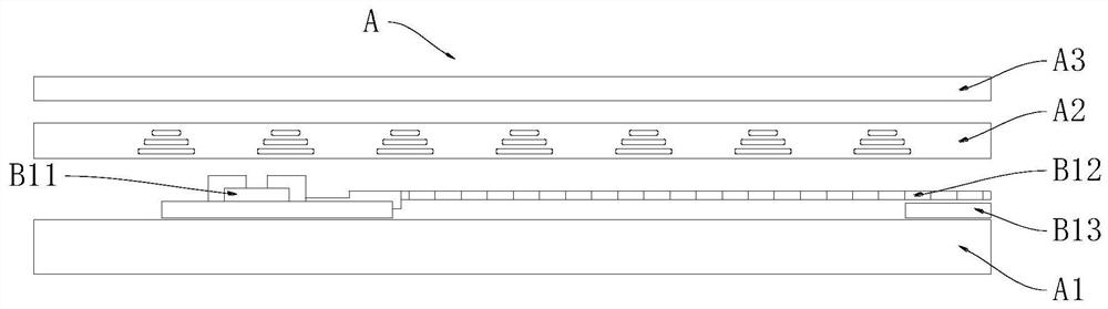
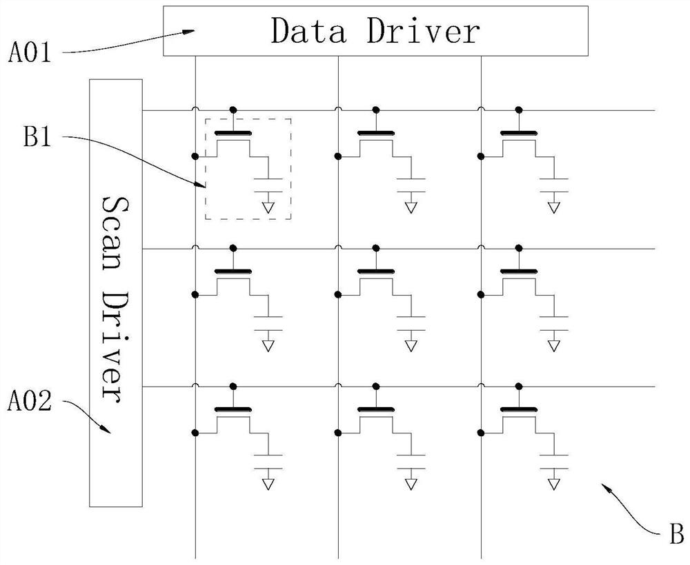
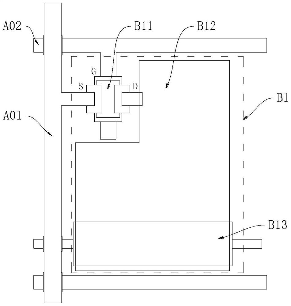
[0040]A built-in LTPS display panel pixel point monitoring system, including a display panel A, the display panel A such asfigure 1 As shown, the panel substrate A1, the liquid crystal layer A2, and the polarizing layer A3 are sequentially included from the inside to the outside. The panel substrate A1 is etched with a pixel point array B of m×n pixels B1, where n is the number of rows, m is the number of columns, such asfigure 2 ,3The pixel point B1 includes a MOSFETB11 and a pixel electrode B12, the source S of the MOSFETB11 is connected to the pixel point data driving line A01, the gate G is connected to the pixel point scanning driving line A02, and the drain D is connected to the pixel electrode B12 , Wherein, a storage capacitor B13 is also provided next to each pixel electrode B12, and its function is similar to that of the pixel electrode B12, and t...


PUM


Abstract

The invention discloses a built-in LTPS display panel pixel point monitoring system, which includes a display panel. The display panel includes a panel substrate, a liquid crystal layer, and a polarizing layer from the inside to the outside, and m×n pixels are etched on the panel substrate. A pixel point array of points, the panel substrate is also provided with a detection and acquisition module, the detection and acquisition module includes a pixel monitoring array and a timing sampling circuit, the pixel monitoring array includes m×n monitoring units, and the monitoring unit and The pixels are in one-to-one correspondence. Beneficial effects: Microscopically detect whether each possible bad pixel is normal, the monitoring effect must be direct and accurate, the monitoring signal of the monitoring unit is compiled and converted into a timing signal flow by the timing sampling circuit, and the self-checking analysis module analyzes Timing information flow, get the pixel dead point result, you can quickly know the location of the bad point.

Description

Technical field[0001]The invention relates to the technical field of LTPS display panel dead pixel detection, in particular to a built-in LTPS display panel pixel point monitoring system.Background technique[0002]Thin film transistor liquid crystal display (TFT-LCD) is a display technology of today's electronic display screens. The light transmission of the liquid crystal layer is controlled by the TFT pixel matrix on the substrate, which specifically includes amorphous silicon (a-Si) and low-temperature polysilicon ( LTPS) Two TFT technologies. Among them, the structure of the LTPS panel includes a bottom light source. On the bottom light source, there are a TFT substrate, a liquid crystal layer, a polarizing layer, and a glass protective layer from the inside to the outside.figure 1 As shown, the TFT substrate is a glass substrate, and its surface is covered with a polysilicon film. The FET (Field Effect Transistor) lattice is etched on the polysilicon film, such asfigure 2 , Non-...

Claims


Application Information

Patent Timeline
Patent Type & Authority Patents(China)
IPC IPC(8): G09G3/36G09G3/00
CPCG09G3/006G09G3/36G09G2330/10G09G2330/12
Inventor 陈新银刘立明
Owner 重庆蓝岸科技股份有限公司
Why Eureka
Try Eureka