Multi-layer PCB structure three-dimensional magnetic field coil

A three-dimensional magnetic field and PCB board technology, which is applied in the direction of coils, measuring magnetic variables, measuring geometric arrangement of magnetic sensing elements, etc., can solve the problems that PCB wiring cannot cross, it is difficult to ensure the consistency of measuring coils, and unfavorable magnetic field measurement differences, etc.

Active Publication Date: 2019-09-13
NAVAL UNIV OF ENG PLA
View PDF19 Cites 2 Cited by
  • Summary
  • Abstract
  • Description
  • Claims
  • Application Information

AI Technical Summary

Problems solved by technology

[0003] Due to the difference in the process of winding coils, it is difficult to ensure the consistency of different measurement coils, which is not conducive to comparing the differences in magnetic field measurements at different spatial positions
Printed circuit board The manufacturing process of the PCB coil is consistent, but the PCB wiring cannot cross, and it is difficult for conventional PCB coils to avoid magnetic field coupling interference in different measurement directions
like figure 1 The double-layer PCB coil, the solid line is the top PCB wiring, and the dotted line is the bottom PCB wiring. It is designed for the measurement of the Z-direction magnetic field, and the coil is located in the XY plane; but there is an induction area for the Y-direction magnetic field between the top layer and the bottom PCB. , so the measured value will contain the coupling interference of the magnetic field in the Y direction; especially, when the magnetic field in the Z direction is small, the coupling interference of the strong magnetic field in the Y direction will make figure 1 The coil test data has a large deviation

Method used


Image

  • Multi-layer PCB structure three-dimensional magnetic field coil
  • Multi-layer PCB structure three-dimensional magnetic field coil
  • Multi-layer PCB structure three-dimensional magnetic field coil

Examples


Embodiment Construction

[0020] The present invention will be further described in detail below in conjunction with the accompanying drawings and specific embodiments to facilitate a clear understanding of the present invention, but they do not limit the present invention.

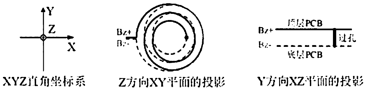
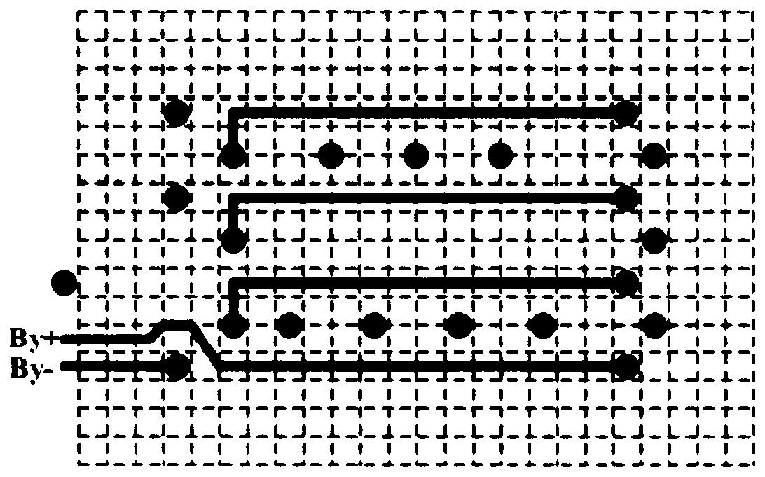
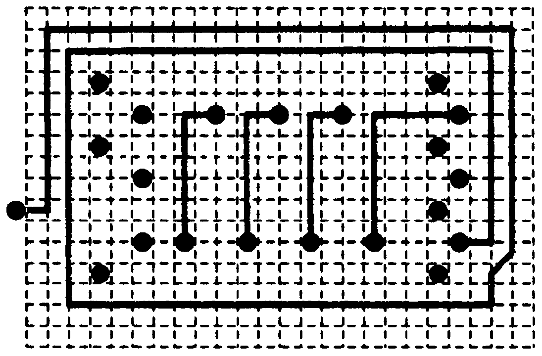
[0021] The three-dimensional magnetic field coil structure of the multilayer PCB structure of the present invention is shown in FIG. 2 . In the figure, the dots are via holes, and the solid lines are PCB wiring; each layer of PCB is located on the XY plane, the X direction is to the right, the Y direction is upward, and the dotted line grid spacing is 1mm; there are six layers of PCB in the Z direction, and the spacing between each layer of PCB 1mm. The specific embodiments of the present invention will be described in detail below in conjunction with the accompanying drawings, which are meant to explain rather than limit the present invention.

[0022] The x-direction measurement coil is wired with Mid-1, Mid-3 and Bottom three-...


PUM


Abstract

The invention provides a multi-layer PCB structure three-dimensional magnetic field coil. The multi-layer PCB structure three-dimensional magnetic field coil is characterized by comprising at least three layers of PCBs, and the multilayer PCBs form three mutually orthogonal measuring coils, the centers of the three coils coincide, and the three-dimensional magnetic field at the same spatial position can be accurately measured; an X-direction measuring coil and a Y-direction coil measuring coil are wired by the top layer, the bottom layer and the middle layer PCBs; the PCB wires on the top layer and the bottom layer form a coil main body, and the coupling area of the measuring coil to the magnetic field in the YZ direction and the magnetic filed in the XZ direction is eliminated through thePCB wire in the middle layer; and the Z direction measuring coil forms a coil main body by the PCB wire in the middle layer, and through the connection sequence and the through hole position of eachlayer of PCB, the coupling area of the measuring coil to the magnetic field in the XY direction is eliminated.

Description

technical field [0001] The invention relates to the field of magnetic field measurement. Specifically, the invention relates to a three-dimensional magnetic field coil with a multilayer PCB structure, which is especially suitable for testing occasions with strong magnetic field and large rate of change, and can be used for three-dimensional space magnetic field distribution measurement of pulsed large current systems. Background technique [0002] Magnetic field measurement often uses Hall elements, magnetoresistive elements, fluxgates or coils. Hall elements, magnetoresistive elements, and fluxgates are only suitable for low-intensity magnetic field measurements, and coils can be used to measure magnetic fields of different strengths. To obtain the three-dimensional characteristics of the high-intensity magnetic field, three mutually orthogonal measuring coils can be used; to distinguish the difference in the magnetic field at different spatial positions, the measuring coil...

Claims


Application Information

Patent Timeline
IPC IPC(8): H01F5/00G01R33/00G01R33/10
CPCG01R33/0005G01R33/10H01F5/003
Inventor 赵治华程龙李建轩张向明李文禄孟进张磊
Owner NAVAL UNIV OF ENG PLA
Why Eureka
Try Eureka