A 10-micron-level high-precision device assembly surface inspection method
A surface inspection and device surface technology, applied in the field of virtual assembly, can solve the problems of increased algorithm estimation time, large number of iterations, etc.
- Summary
- Abstract
- Description
- Claims
- Application Information
AI Technical Summary
Problems solved by technology
Method used
Image

Examples
Embodiment Construction
[0032] The present invention will be described in detail below in conjunction with the implementations shown in the drawings, but it should be noted that these implementations are not limitations of the present invention, and those of ordinary skill in the art based on the functions, methods, or structural changes made by these implementations Equivalent transformations or substitutions all fall within the protection scope of the present invention.
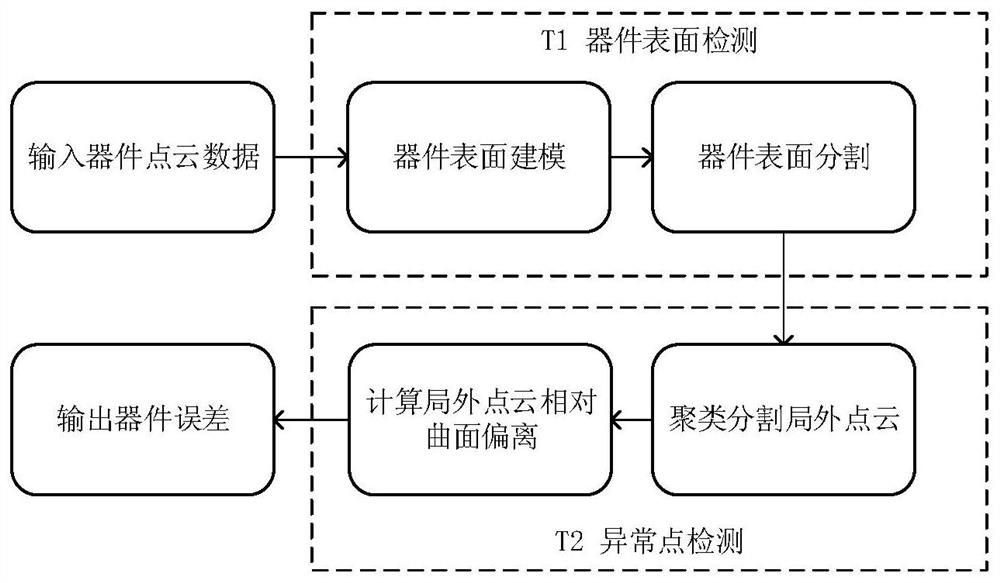
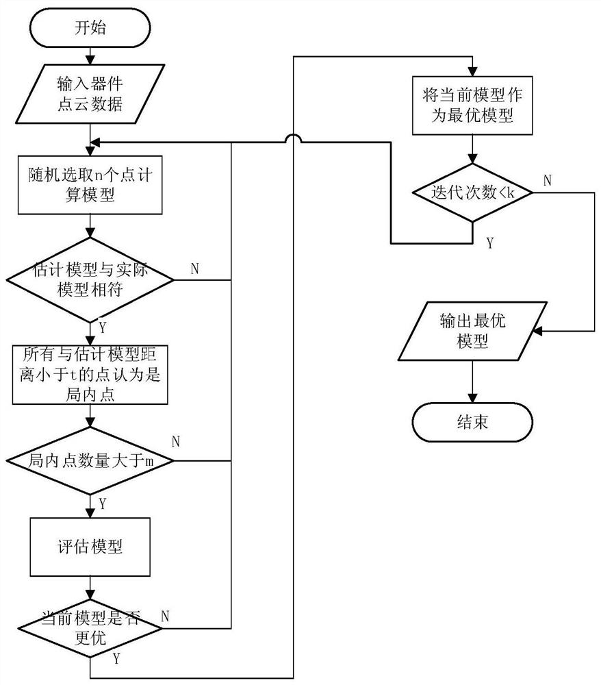
[0033] For the assembly model reconstructed from the 3D point cloud in the virtual assembly environment, the surface of the assembleable device will be partially deformed (convex). When the size of the assembled device is appropriate, these deformed areas will lead to assembly failure. Location. The main function of this method is to find the highest convex distance from the assembly surface. This method divides the point cloud data into two sets, one is the set of internal points, and the other is the set of external points, usi...
PUM
 Abstract
Description
Claims
Application Information