Nested micro-trap structure and preparation method for suppressing secondary electron emission

A technology of secondary electron emission and secondary electrons, which is applied in the field of physical electronics, can solve the problems of limited suppression effect, achieve the effect of increasing micro-discharge threshold, strengthening suppression, and suppressing the total output

Inactive Publication Date: 2020-06-16
BEIJING INSTITUTE OF TECHNOLOGYGY +1
View PDF3 Cites 0 Cited by
  • Summary
  • Abstract
  • Description
  • Claims
  • Application Information

AI Technical Summary

Problems solved by technology

[0006] In order to solve the problem that the suppression effect of the surface trap structure in the prior art is limited due to the multi-level multiplication effect of electrons in the trap, the nested micro-trap structure and preparation method for suppressing secondary electron emission disclosed by the present invention are to be solved The technical problem is: effectively suppress the multi-level multiplication effect produced by the secondary electron emission and re-emission in the trap structure, so as to improve the total secondary electron emission suppression effect on the surface of the material, and provide a preparation method for the nested micro-trap structure

Method used


Image

  • Nested micro-trap structure and preparation method for suppressing secondary electron emission
  • Nested micro-trap structure and preparation method for suppressing secondary electron emission
  • Nested micro-trap structure and preparation method for suppressing secondary electron emission

Examples


Embodiment 1

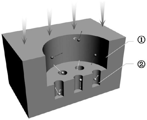
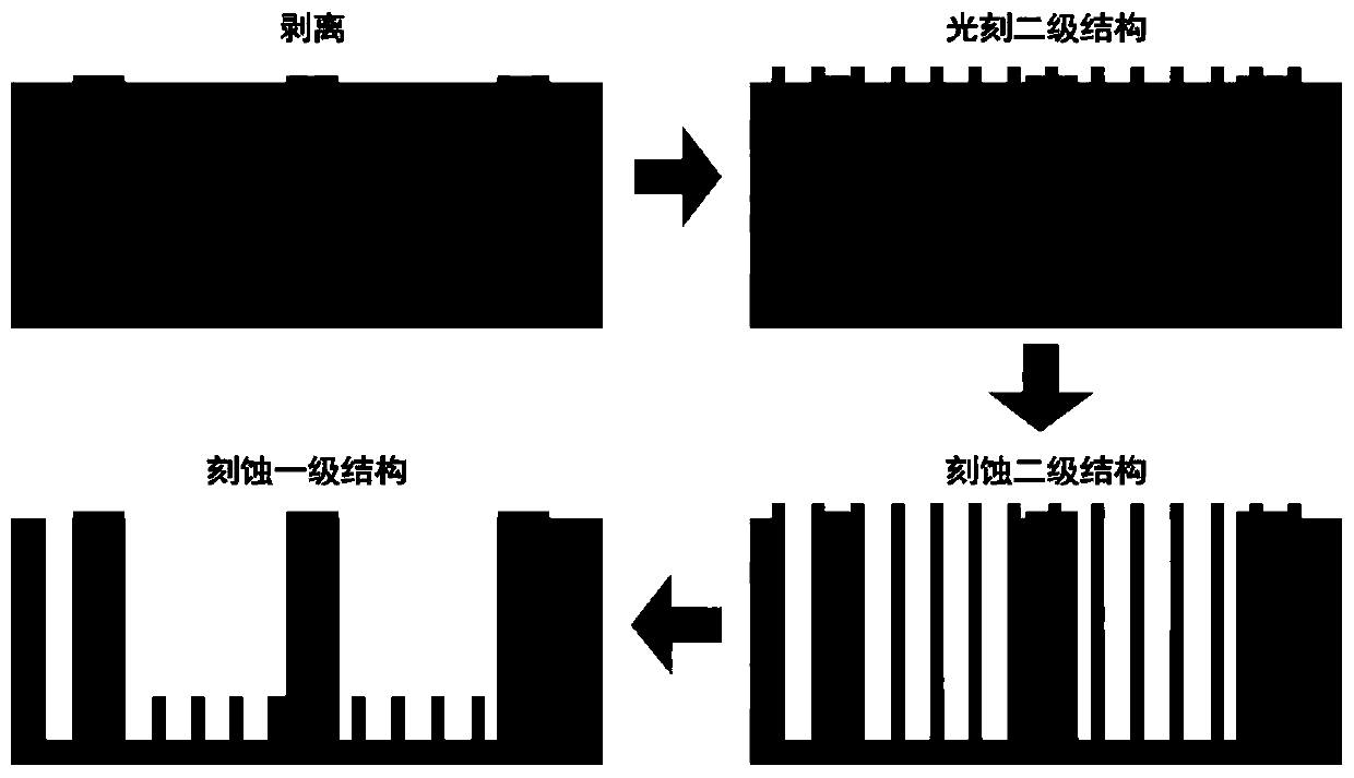
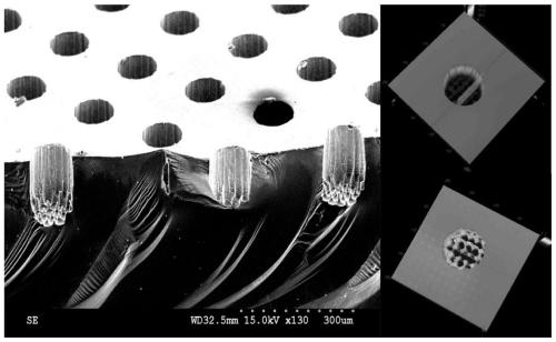
[0027] Such as figure 1 As shown, the nested micro-trap structure disclosed in this embodiment for suppressing secondary electron emission is a double-nested hole structure, and includes several second-level small hole 1 structures in the first-level large hole 1. The first-level large hole 1 is used as the primary trap, and several secondary small hole 1 structures are used as nested traps. The number of structures of the plurality of secondary small holes 1 is determined according to the structural size and duty cycle of the secondary small holes 1 . The overall two-dimensional nested trap structure is configured on the silicon base material, the configuration is a double nested hole structure, and metal sputtering is performed on the double nested hole structure to form a nanoscale film.

[0028] The working method of the nested micro-trap structure for suppressing secondary electron emission disclosed in this embodiment is: when a single initial incident electron is irrad...


PUM


Abstract

The invention discloses a nested micro-trap structure for inhibiting secondary electron emission and a preparation method, and relates to the field of physical electronics. The nested micro-trap structure for inhibiting the secondary electron emission is of a double nested hole structure, a plurality of secondary small hole structures are contained in a primary large hole, the primary large hole serves as a primary trap, and the multiple secondary small hole structures serve as nested traps; and the integral two-dimensional nested trap structure is constructed on a substrate material and is ofthe double nested hole structure, and metal sputtering is carried out on the double nested hole structure so as to form a nano-scale membrane. The invention further discloses the preparation method for the nested micro-trap structure. According to the nested micro-trap structure and the preparation method, the multi-stage multiplication effect generated by secondary electron emission and re-emission in the trap structure can be effectively inhibited, and therefore the total secondary electron emission inhibition effect on the surface of the material is improved. The invention provides the preparation method for the nested micro-trap structure.

Description

technical field [0001] The invention relates to the related field of physical electronics, in particular to a surface microstructure capable of strongly and effectively suppressing secondary electron emission on the surface of a material and a preparation method thereof. Background technique [0002] my country's spacecraft payload urgently needs to develop towards integration and high power. However, in the harsh space environment, it will also lead to the intensification of some special effects in space. The micro-discharge effect of space high-power microwave components is the first problem. [0003] The space micro-discharge effect is also called the secondary electron multiplication effect, which refers to the high-power microwave components at 1×10 -3 It is a resonant discharge phenomenon generated when transmitting high-power microwave signals at Pa or lower pressure. That is, the electrons in the high-power microwave passive devices and component structural gaps in...

Claims


Application Information

Patent Timeline
Patent Type & Authority Patents(China)
IPC IPC(8): C23C14/16C23C14/02B82Y30/00B82Y40/00
CPCB82Y30/00B82Y40/00C23C14/02C23C14/16
Inventor 李东封国宝王琪何鋆胡天存
Owner BEIJING INSTITUTE OF TECHNOLOGYGY
Why Eureka
Try Eureka