

Band-pass filter
A technology of band-pass filter and resonator, applied in the direction of waveguide type device, waveguide, resonator, etc., can solve the problem of unrealistic and achieve the effect of suppressing inconsistency
- Summary
- Abstract
- Description
- Claims
- Application Information
AI Technical Summary
Problems solved by technology
Method used
Image

Examples
no. 1 approach 〕
[0026] (Structure of bandpass filter 1)
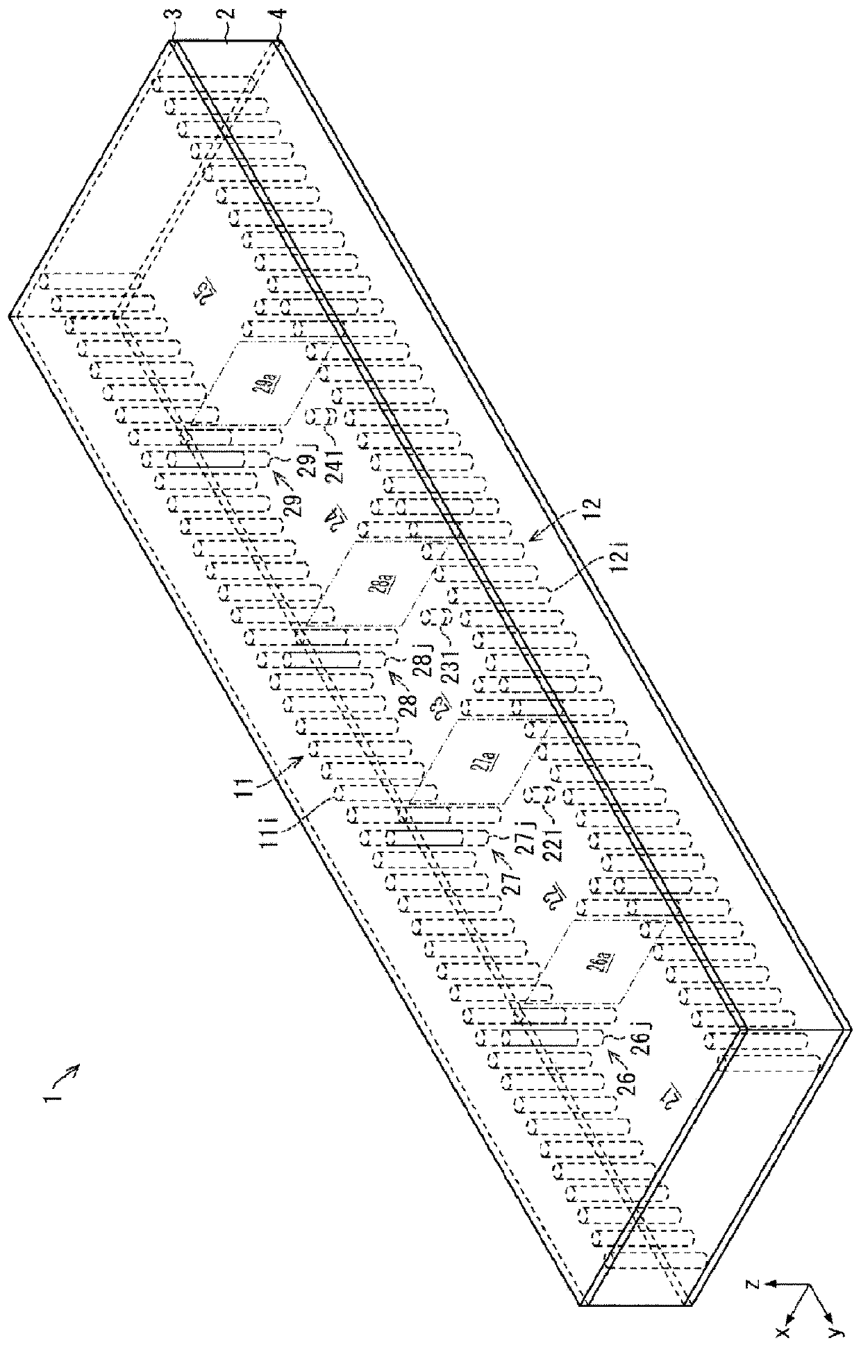
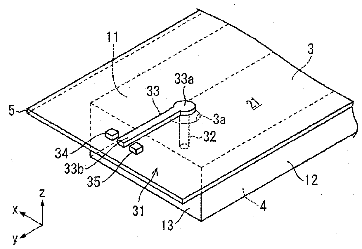
[0027] refer to figure 1 and figure 2 A bandpass filter (BPF, BandPassFilter) according to the first embodiment of the present invention will be described. figure 1 It is a perspective view of BPF1 concerning this embodiment. figure 2 It is a perspective view of the conversion part 31 with which BPF1 is equipped.
[0028] Such as figure 1 As shown, BPF 1 includes substrate 2 made of a dielectric material, conductive layer 3 and conductive layer 4 as a pair of conductive layers, and column wall 11 and column wall 12 .
[0029] The substrate 2 is a plate-like member made of a dielectric. Hereinafter, among the six surfaces constituting the substrate 2 , the two surfaces with the largest areas are referred to as main surfaces of the substrate 2 . In this embodiment, quartz is used as the dielectric material constituting the substrate 2 , but other dielectric materials (for example, resins such as Teflon (registered trademark) resi...
no. 2 approach 〕
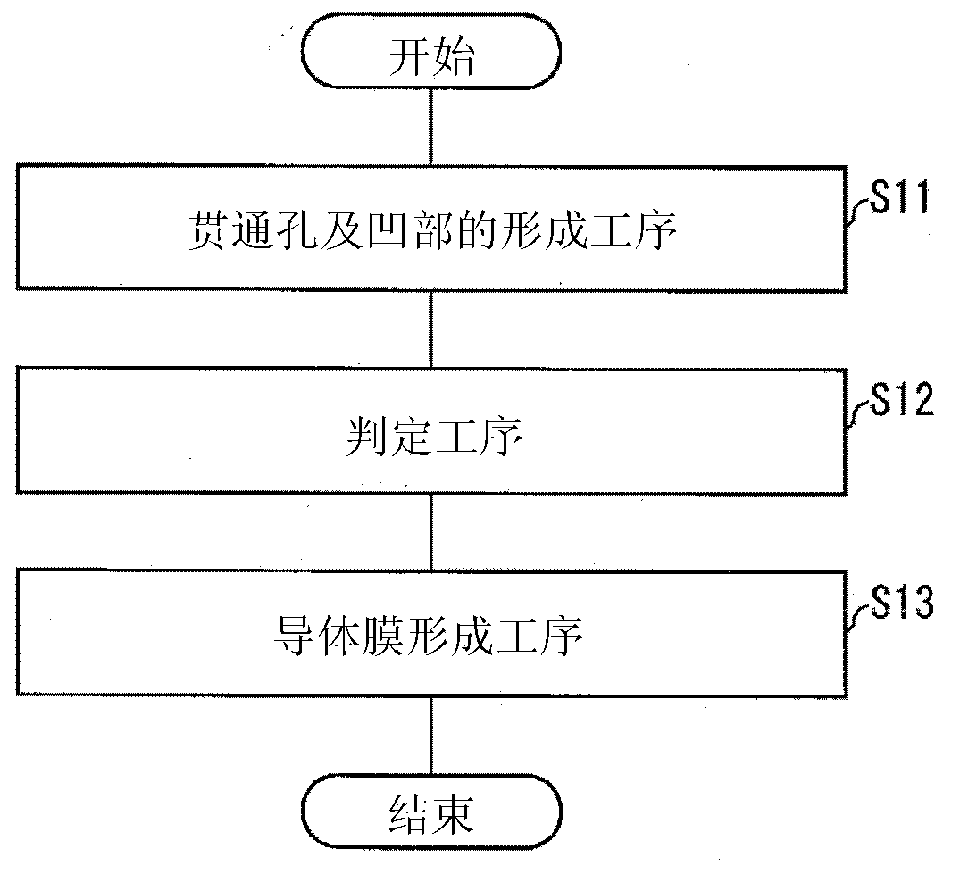
[0074] refer to image 3 A method of manufacturing the bandpass filter according to the second embodiment of the present invention will be described. image 3 It is a flowchart of the manufacturing method of the bandpass filter which concerns on this embodiment. This manufacturing method mainly involves figure 1 The step of forming the recesses 221 , 231 , and 241 and the step of forming a conductor film on the inner walls of the recesses 221 , 231 , and 241 in the manufacturing method of the BPF 1 shown are shown.
[0075] (Manufacturing method of BPF1)
[0076] Such as image 3 As shown, this manufacturing method includes the forming step S11 of the through-hole and the concave portion, the determining step S12, and the forming step S13 of the conductor film.
[0077] The forming step S11 of through-holes and recesses is a step of forming (1) a plurality of through-holes for forming conductor posts 11i, 12i, 26j, 27j, 28j, and 29j on the substrate 2 based on a predetermi...
no. 3 approach 〕
[0088] refer to Figure 4 BPF 101 according to the third embodiment of the present invention will be described. Figure 4 It is a perspective view of BPF101. In addition, in Figure 4 In order to easily observe the structure of the four recesses (recesses 1221-1224, 1231-1234, 1241-1244) formed in each resonator 122-124, each column wall 111, 112 and each partition wall 126 constituting each resonator Numerals to 129 are schematically shown not as columnar waveguides using columnar walls but as rectangular waveguides using imaginary planar walls. In addition, each column wall 111,112 and each partition wall 126-129 are not shown as the wall which has thickness, but are shown by the imaginary surface.
[0089] BPF101 by targeting figure 1 The BPF1 shown is obtained by adding another concave portion. In this embodiment, after clarifying the correspondence relationship between BPF101 and BPF1, the difference between BPF101 and BPF1 will be mainly described.
[0090] BPF 101...
PUM
 Abstract
Description
Claims
Application Information