Array substrate, preparation method thereof and display device
A technology of array substrates and substrates, which is applied in the direction of electrical components, electric solid devices, circuits, etc., can solve the problems of poor ink dripping position, etc., achieve the effect of reducing poor display, simple method, and convenient for mass production
- Summary
- Abstract
- Description
- Claims
- Application Information
AI Technical Summary
Problems solved by technology
Method used
Image
Examples
Embodiment 1
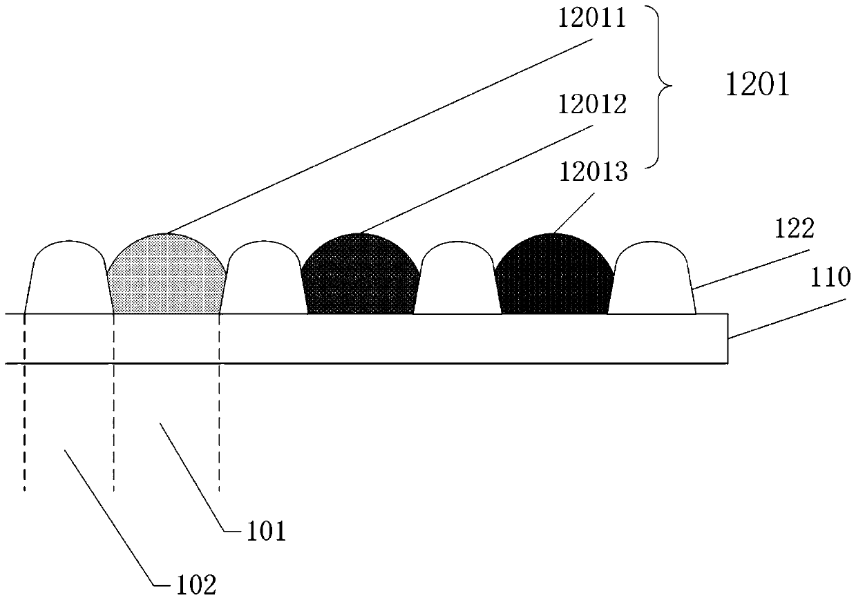
[0034] Such as image 3 As shown, in this embodiment, the array substrate 10 of the present invention includes a substrate 110 and a pixel definition layer 120 .
[0035] The array substrate 10 includes a light-emitting area 101 and a non-light-emitting area 102 surrounding the light-emitting area 101 , and the light-emitting area 101 is used to provide a display image.
[0036] Such as Figure 4 As shown, the pixel definition layer 120 is disposed on the substrate 110, and its material is made of hydrophobic and oleophobic materials, such as fluorine-containing materials. In order to receive the ink used to emit light, the pixel definition layer 120 is provided with several openings 121 corresponding to the light emitting area 101, wherein the pixel definition layer 120 between adjacent openings 121 is a barrier wall 122 In the prior art, the inkjet printing method is generally used to drop the ink into the opening 121, but due to the improvement of the resolution and the r...
Embodiment 2
[0038] In this embodiment, the array substrate 10 of the present invention includes a substrate 110 and a pixel definition layer 120 .
[0039] The array substrate 10 includes a light-emitting area 101 and a non-light-emitting area 102 surrounding the light-emitting area 101 , and the light-emitting area 101 is used to provide a display image.
[0040] The pixel definition layer 120 is disposed on the substrate 110 and its material is made of hydrophobic and oleophobic materials, such as fluorine-containing materials. Such as Figure 4 As shown, in order to receive the ink for emitting light, the pixel definition layer 120 is provided with several openings 121 corresponding to the light emitting area 101, wherein the pixel definition layer 120 between adjacent openings 121 is For the retaining wall 122, in the prior art, ink is generally dropped into the opening 121 by means of inkjet printing, but due to the improvement of the resolution and the reduction of the pixel size, ...
PUM
| Property | Measurement | Unit |
|---|---|---|
| width | aaaaa | aaaaa |
| depth | aaaaa | aaaaa |
Abstract
Description
Claims
Application Information


