Eureka AIR delivers breakthrough ideas for toughest innovation challenges, trusted by R&D personnel around the world.

Three-dimensional storage device having source structure and method for forming the same

A storage device and source technology, applied in the direction of semiconductor devices, electrical components, circuits, etc.

Active Publication Date: 2019-12-27
YANGTZE MEMORY TECH CO LTD
View PDF6 Cites 4 Cited by
  • Summary
  • Abstract
  • Description
  • Claims
  • Application Information

AI Technical Summary

Problems solved by technology

However, as the feature size of memory cells approaches the lower limit, planar processes and fabrication techniques become challenging and expensive
As a result, storage densities for planar memory cells approach the upper limit

Method used


Image

  • Three-dimensional storage device having source structure and method for forming the same
  • Three-dimensional storage device having source structure and method for forming the same
  • Three-dimensional storage device having source structure and method for forming the same

Examples


Embodiment Construction

[0028] While specific configurations and arrangements are discussed, it should be understood that this is done for illustrative purposes only. A person skilled in the relevant art will recognize that other configurations and arrangements may be used without departing from the spirit and scope of the present disclosure. It will be apparent to those skilled in the relevant art that the present disclosure may also be employed in various other applications.

[0029] It is worth noting that references in this specification to "one embodiment," "an embodiment," "example embodiments," "some embodiments," etc. indicate that the described embodiments may include the particular feature, structure, or characteristic. , but each embodiment may not necessarily include specific features, structures or characteristics. Moreover, such phrases are not necessarily referring to the same embodiment. Further, when a particular feature, structure, or characteristic is described in conjunction wit...


PUM


Abstract

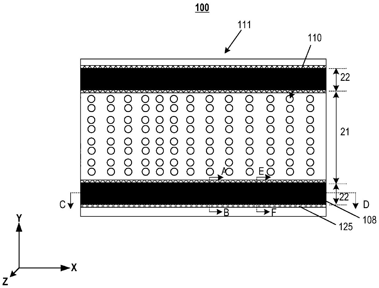
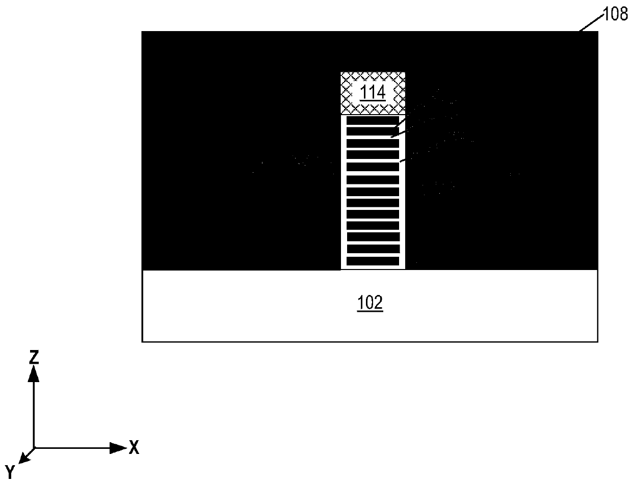
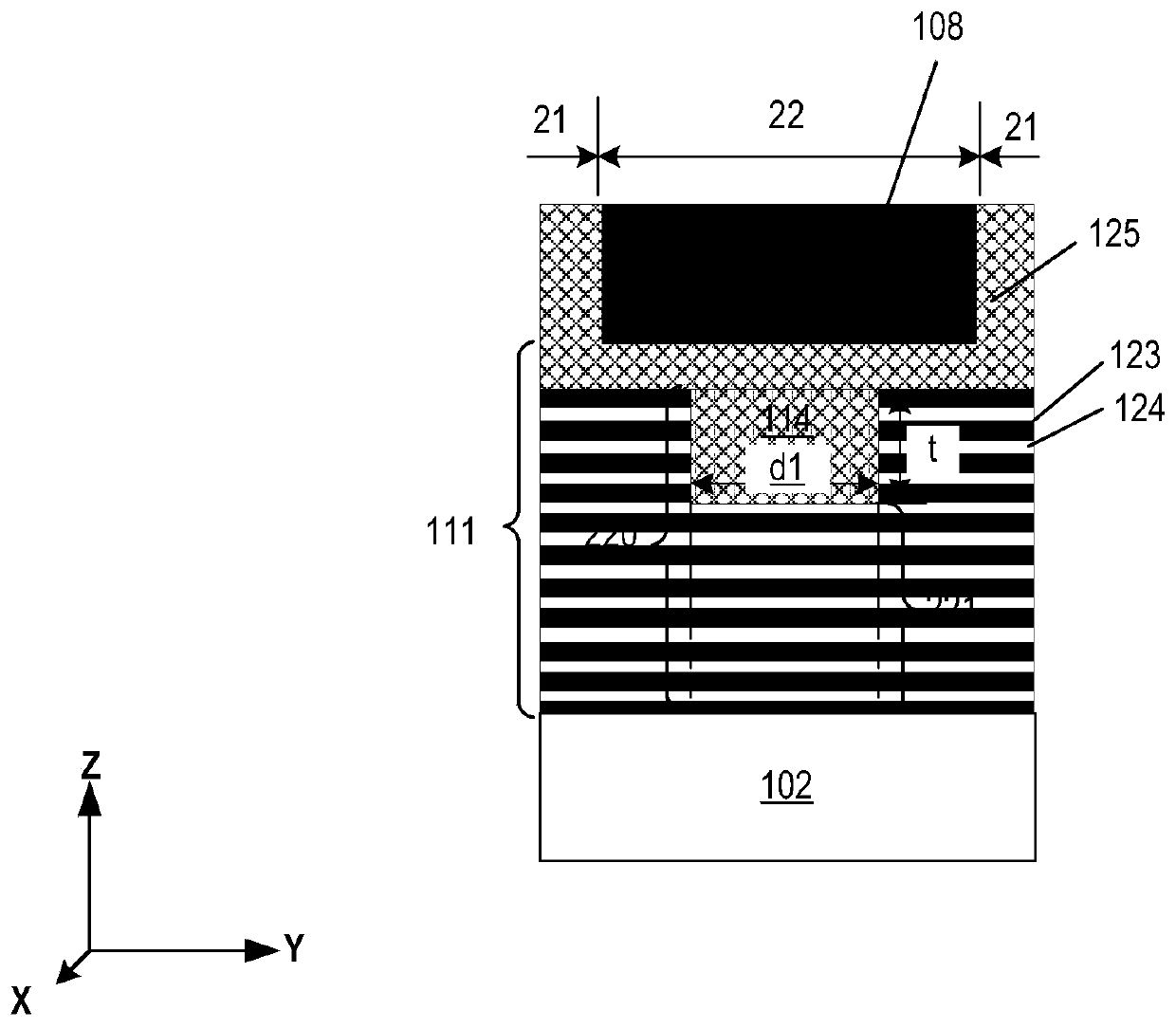
Embodiments of structures and methods for forming a three-dimensional (3D) storage device are provided. In one example, a 3D storage device includes a storage stack over a substrate, a plurality of channel structures, and a source structure. The memory stack includes a plurality of interleaved conductor layers and a plurality of insulating layers. A plurality of channel structures extends vertically in the memory stack. A source structure extends in the memory stack. The source structure includes a plurality of source contacts, each source contact in a respective insulating structure. At leasttwo of the plurality of source contacts are in contact with each other and are conductively connected to each other.

Description

technical field [0001] Embodiments of the present disclosure relate to a three-dimensional (3D) memory device having a source structure of reduced resistance and a method for forming the 3D memory device. Background technique [0002] Planar memory cells are scaled to smaller sizes by improving process technology, circuit design, programming algorithms, and manufacturing processes. However, as the feature size of memory cells approaches the lower limit, planar processes and fabrication techniques become challenging and expensive. As a result, storage density for planar memory cells approaches an upper limit. [0003] 3D memory architectures can address density limitations in planar memory cells. A 3D memory architecture includes a memory array and peripherals for controlling signals to and from the memory array. Contents of the invention [0004] Embodiments of 3D storage devices and methods for forming 3D storage devices are provided. [0005] In one example, a 3D mem...

Claims


Application Information

Patent Timeline
Patent Type & Authority Applications(China)
IPC IPC(8): H01L27/1157H01L27/11582H01L29/417H01L21/28H10B43/35H10B69/00H10B43/10H10B43/27H10B43/50
CPCH01L29/41725H01L29/401H01L29/41741H10B43/35H10B43/27H10B43/10H10B43/50H01L21/02164H01L21/0228H01L21/31116H01L21/76802H01L21/76831H01L21/76834H01L21/76877
Inventor 黄攀徐伟严萍徐文祥霍宗亮周文斌夏季
Owner YANGTZE MEMORY TECH CO LTD
Why Eureka
Eureka Blog
Learn More