PCB

A PCB board and area technology, applied in the electronic field, to achieve the effect of improving signal quality, improving integrity, and ensuring correct transmission

Inactive Publication Date: 2020-01-07
GOERTEK OPTICAL TECH CO LTD
View PDF4 Cites 0 Cited by
  • Summary
  • Abstract
  • Description
  • Claims
  • Application Information

AI Technical Summary

Problems solved by technology

[0006] In view of the above problems, the purpose of the present invention is to provide a PCB board to solve the problems of how to offset the jump of impedance line impedance, ensure correct transmission, and improve the signal quality of transmission signals.

Method used


Image

  • PCB
  • PCB
  • PCB

Examples


Embodiment Construction

[0028] Aiming at the aforementioned problem of how to offset the jump of impedance line impedance, ensure correct transmission, and improve the signal quality of the transmitted signal, it has become an urgent problem to be solved at present. The present invention provides a new PCB board to solve the above problem.

[0029] Specific embodiments of the present invention will be described in detail below in conjunction with the accompanying drawings.

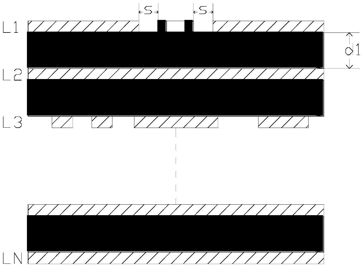
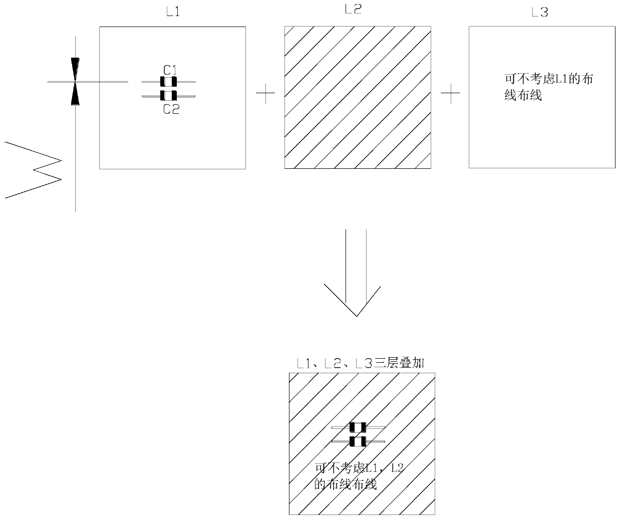
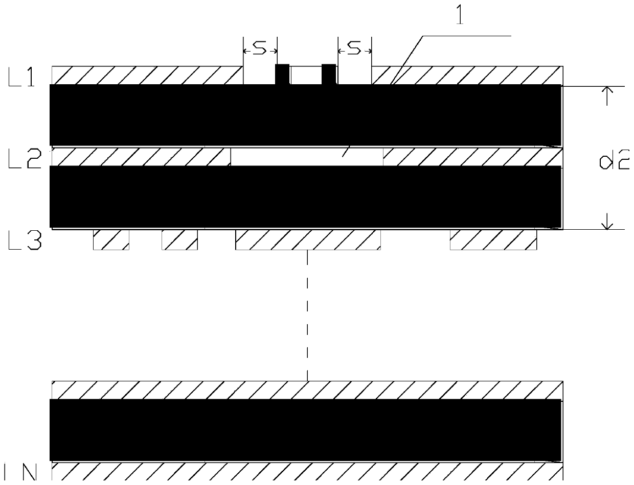
[0030] In order to illustrate the structure of the PCB board provided by the present invention, diagram 2-1 and Figure 2-2 The structure of the PCB board is exemplarily marked from different angles. specifically, diagram 2-1 shows a PCB layout cross-sectional structure according to an embodiment of the present invention; Figure 2-2 The layout of each layer of the PCB and its superimposed structure according to the embodiment of the present invention are shown.

[0031] Such as Figure 2-1 to Figure 2-2 Commonly shown, th...


PUM


Abstract

The invention provides a PCB. The PCB comprises a top layer, a bottom layer and at least two middle layers arranged between the top layer and the bottom layer, wherein the middle layer comprises a second layer and a third layer, the top layer is provided with a pair of series capacitors on a differential line, the area of the series capacitor where the top layer is located is a capacitor series distribution area, a wiring forbidding area is arranged at the position, corresponding to the capacitor series distribution area, of the second layer, the wiring forbidding area is larger than the capacitor series distribution area, a GND attribute area is arranged at the position, corresponding to the wiring forbidding area, of the third layer, and the GND attribute area provides reference for thedifferential line of the top layer. The PCB is advantaged in that problems of how to counteract hopping of impedance of an impedance line, guarantee correct transmission, improve the signal quality ofa transmission signal and the like can be solved.

Description

technical field [0001] The invention relates to the field of electronic technology, and more specifically, relates to a PCB board with signal integrity and reliability that can be widely used in packaging parts. Background technique [0002] Nowadays, electronic products are developing towards thinner and lighter, and the speed of replacement is also increasing. Functional requirements are becoming more and more abundant. Requirements for important electronic components of electronic products, supports for electronic components, and PCBs for carriers of electrical connections for electronic components It is also becoming more and more stringent, and the requirements for the integrity of PCB signals and product reliability are getting higher and higher. [0003] exist Picture 1-1 and Figure 1-2 In the shown embodiment, the PCB board is N layers, in which the conductive layers are separated by an insulating layer, S is the distance between the border of the series capacitor...

Claims


Application Information

Patent Timeline
IPC IPC(8): H05K1/02
CPCH05K1/0213H05K1/0216H05K1/0298
Inventor 马菲菲
Owner GOERTEK OPTICAL TECH CO LTD
Why Eureka
Try Eureka