
A planarization treatment method for ultra-thick film

A processing method and flattening technology, applied in the field of flattening processing of ultra-thick adhesive films, can solve the problems of reduced product reliability, large thickness of metal lines, and high process difficulty, and achieves the goal of reducing the number of times and increasing the uniformity of coverage. Effect

Active Publication Date: 2022-05-17
浙江集迈科微电子有限公司
View PDF0 Cites 0 Cited by
  • Summary
  • Abstract
  • Description
  • Claims
  • Application Information

AI Technical Summary

Problems solved by technology

[0004] However, in practical applications, for some special processes, the thickness of the metal wire is relatively large. For coating the PI layer to cover the metal wire, the process becomes more and more difficult, especially for the metal wire with a height of more than 30um. When the PI layer is in the After passing over the surface of the metal wire during spin coating, it often cannot continue to cover the back of the metal wire, but directly flies out under the action of centripetal force.
This process often needs to coat three layers of PI to barely cover the two measuring surfaces of the circuit at the same time, which increases the cost and reduces the reliability of the product.

Method used


Image

  • A planarization treatment method for ultra-thick film
  • A planarization treatment method for ultra-thick film
  • A planarization treatment method for ultra-thick film

Examples


Embodiment 1

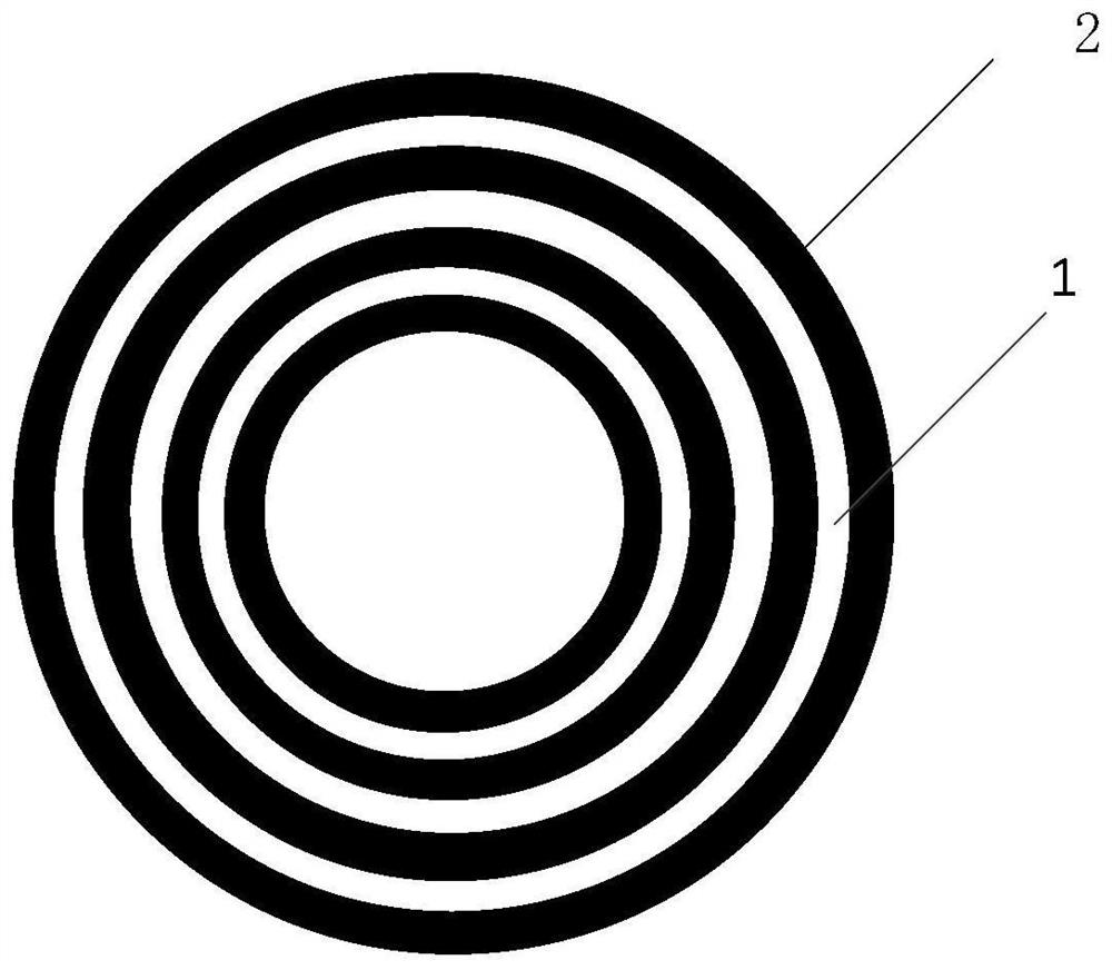
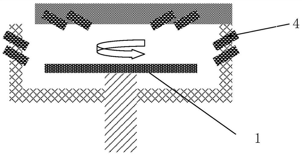
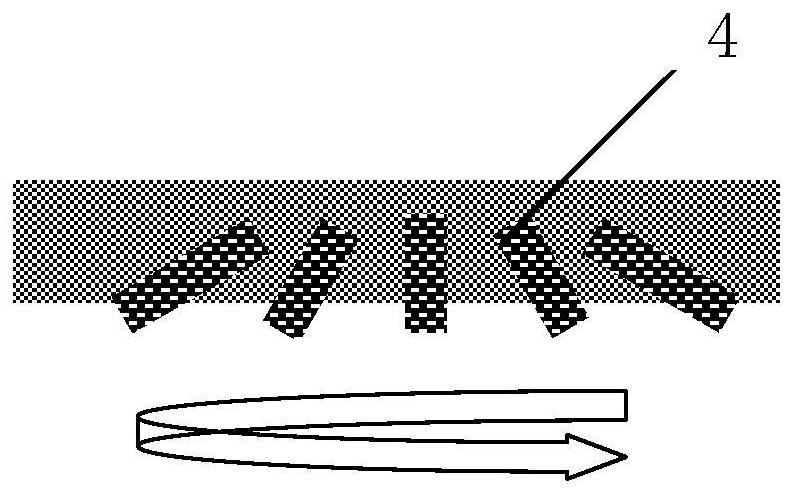
[0033] Such as Figure 1 to Figure 11 Shown, a kind of planarization treatment method of super thick adhesive film specifically comprises the following steps:

[0034] 101) Preliminary spraying step: heating the bottom of the circuit carrier 1 with the circuit metal wire 2 at 50 to 150 degrees; the height of the circuit metal wire 2 is between 10um and 200um, and the width is between 1um and 1000um. The circuit metal wire 2 itself has a one-layer or multi-layer structure, and its material is a mixture of one or more of titanium, copper, aluminum, silver, palladium, gold, thallium, tin, and nickel. Apply the photoresist 3 on the upper surface of the circuit carrier 1 by direct pasting process, and let it stand for a period of time, the rest time is between 10 seconds and 100 seconds; then rotate the coated photoresist 3, and the speed is controlled at 100 revolutions to 10,000 revolutions per second; wherein, the heating method includes infrared heating to directly heat the ph...


PUM


Abstract

The invention discloses a method for planarizing an ultra-thick adhesive film, which specifically comprises the following steps: 101) a preliminary spraying step, 102) a glue-coating step, 103) a step of preparing an adhesive film, and 104) a step of preparing an ultra-thick adhesive film; The invention provides an ultra-thick adhesive film planarization treatment method with an ultra-thick protective film and high yield.

Description

technical field [0001] The invention relates to the technical field of semiconductors, in particular to a method for planarizing an ultra-thick adhesive film. Background technique [0002] Wafer-level packaging technology is the most widely used technology in the field of advanced packaging, especially for consumer products. Wafer-level packaging is widely used in mobile electronic devices due to its small size, light weight, and thin thickness. on micro-functional devices. [0003] The processes generally involved in wafer-level packaging include dielectric layer coating, circuit layout, and interconnection solder ball implantation. It can be completely covered by the dielectric layer to protect the circuit from corrosion and at the same time insulate the upper and lower metal layers. [0004] However, in practical applications, for some special processes, the thickness of the metal wire is relatively large. For coating the PI layer to cover the metal wire, the process be...

Claims


Application Information

Patent Timeline
Patent Type & Authority Patents(China)
IPC IPC(8): G03F7/16H01L21/56
CPCG03F7/162G03F7/168H01L21/56
Inventor 郁发新冯光建高卫斌马飞程明芳
Owner 浙江集迈科微电子有限公司
Learn More