Semiconductor device

a semiconductor and device technology, applied in semiconductor devices, instruments, electrical devices, etc., can solve the problems of reducing the aperture ratio of a pixel and degrading the display quality of an image, and achieve the effect of improving the aperture ratio

Active Publication Date: 2014-02-06
SEMICON ENERGY LAB CO LTD
View PDF8 Cites 82 Cited by
  • Summary
  • Abstract
  • Description
  • Claims
  • Application Information

AI Technical Summary

Benefits of technology

[0032]According to one embodiment of the present invention, a semiconductor device including...

Problems solved by technology

However, when the area of a light-blocking conductive film is increased to increase the area of a portion where a pair of...

Method used


Image

  • Semiconductor device
  • Semiconductor device
  • Semiconductor device

Examples


embodiment 1

[0089]In this embodiment, a semiconductor device of one embodiment of the present invention will be described with reference to drawings. Note that in this embodiment, a semiconductor device of one embodiment of the present invention will be described taking a liquid crystal display device as an example.

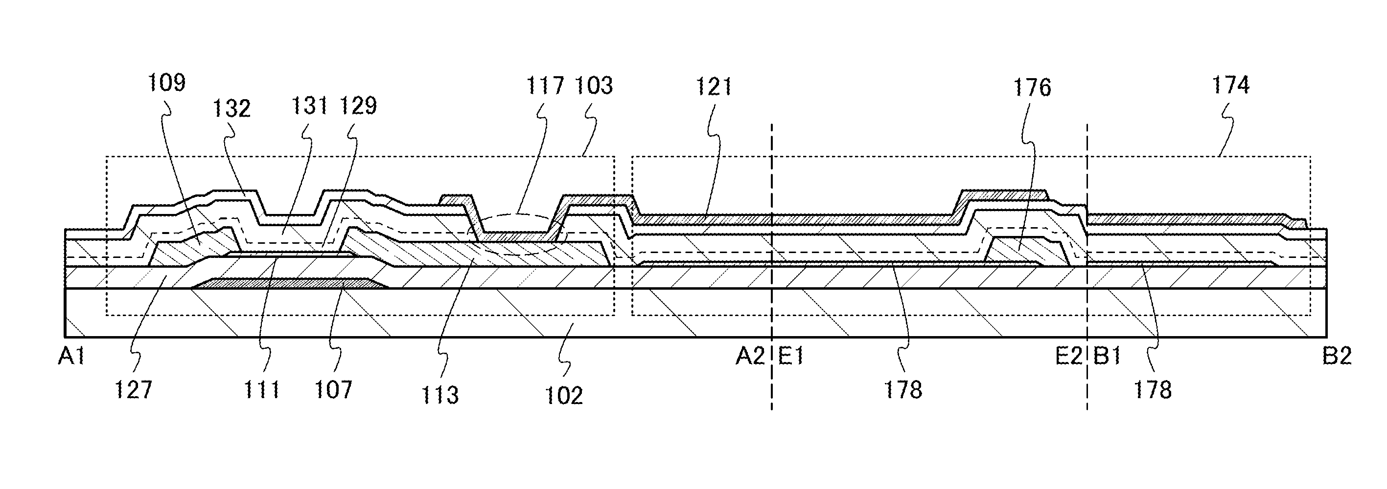
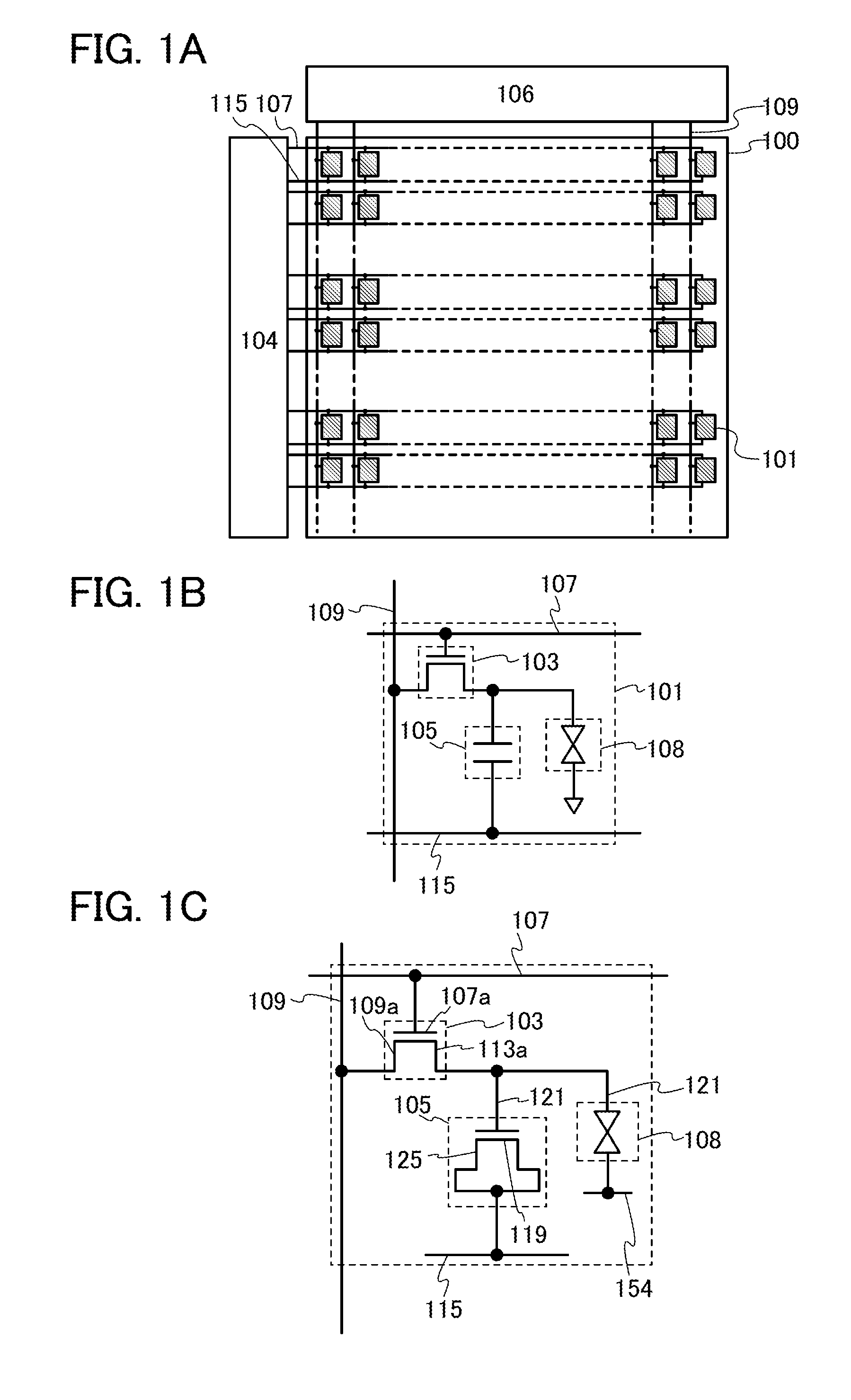
[0090]FIG. 1A illustrates an example of a semiconductor device. The semiconductor device in FIG. 1A includes a pixel portion 100, a scan line driver circuit 104, a signal line driver circuit 106, m scan lines 107 which are arranged in parallel or substantially in parallel and whose potentials are controlled by the scan line driver circuit 104, and n signal lines 109 which are arranged in parallel or substantially in parallel and whose potentials are controlled by the signal line driver circuit 106. Further, the pixel portion 100 includes a plurality of pixels 101 arranged in a matrix. Furthermore, capacitor lines 115 arranged in parallel or substantially in parallel are provided alon...

modification example 1

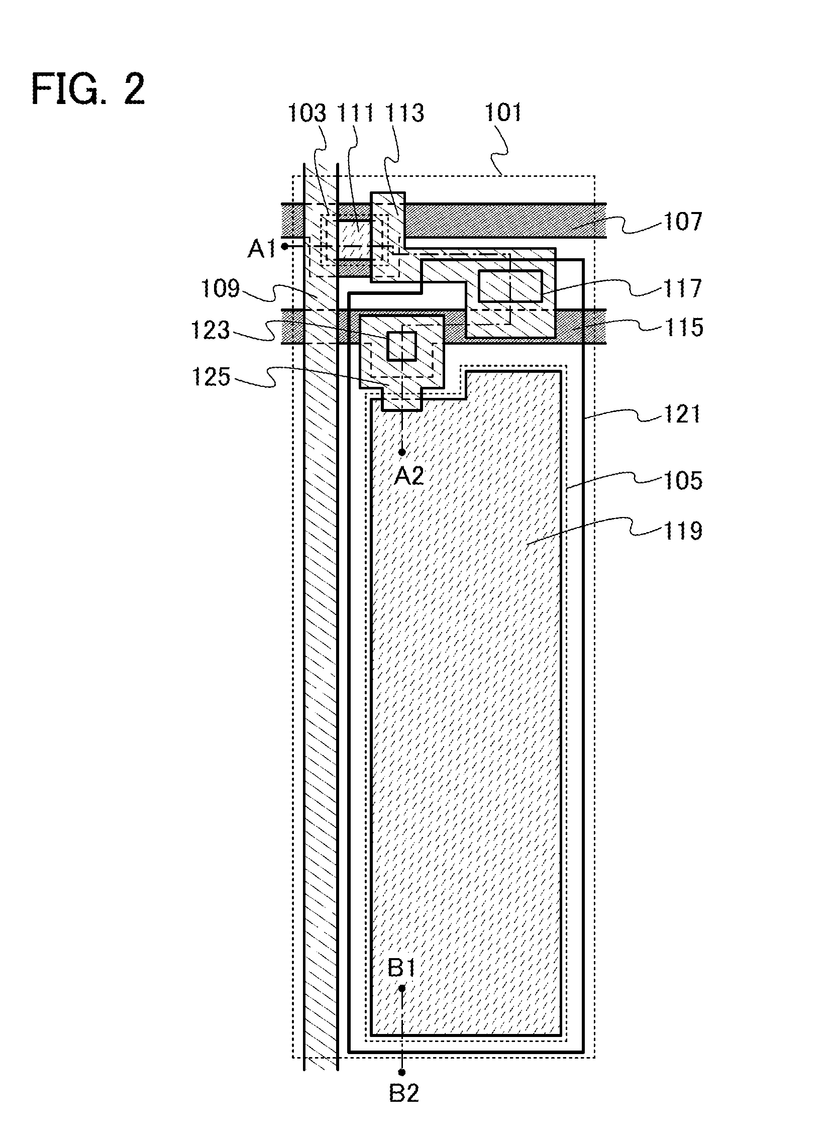
[0192]In the semiconductor device of one embodiment of the present invention, connection of the capacitor line and the semiconductor film serving as one electrode of the capacitor can be changed as appropriate. For example, to improve the aperture ratio, a structure where the semiconductor film is in direct contact with the capacitor line without the conductive film interposed therebetween can be employed. Specific examples of the structure will be described with reference to FIG. 6 and FIG. 7. Here, only a capacitor 145 different from the capacitor 105 described with reference to FIG. 2 and FIG. 3 will be described. FIG. 6 is a top view of a pixel 141, and FIG. 7 is a cross-sectional view taken along dashed-dotted lines A1-A2 and B1-B2 in FIG. 6.

[0193]In the pixel 141, the semiconductor film 119 functioning as one electrode of the capacitor 145 is in direct contact with the capacitor line 115 through an opening 143. Unlike in the capacitor 105 in FIG. 3, the semiconductor film 119 ...

modification example 2

[0195]In the semiconductor device of one embodiment of the present invention, the conductive film which electrically connects the capacitor line and the semiconductor film serving as one electrode of the capacitor can be changed as appropriate. For example, to reduce contact resistance between the semiconductor film and the conductive film, the conductive film can be provided in contact with the semiconductor film along the outer periphery thereof. Specific examples of the structure will be described with reference to FIG. 9 and FIGS. 10A and 10B. Here, only a conductive film 167 different from the conductive film 125 described with reference to FIG. 2 and FIG. 3 will be described. FIG. 9 is a top view of a pixel 161, FIG. 10A is a cross-sectional view taken along dashed-dotted lines A1-A2 and B1-B2 in FIG. 9, and FIG. 10B is a cross-sectional view taken along dashed-dotted line D1-D2 in FIG. 9.

[0196]In the pixel 161, the conductive film 167 is in contact with the semiconductor film...


PUM


Abstract

To provide a semiconductor device including a capacitor whose charge capacity is increased without reducing the aperture ratio. The semiconductor device includes a transistor including a light-transmitting semiconductor film, a capacitor where a dielectric film is provided between a pair of electrodes, an insulating film provided over the light-transmitting semiconductor film, and a light-transmitting conductive film provided over the insulating film. In the capacitor, a metal oxide film containing at least indium (In) or zinc (Zn) and formed on the same surface as the light-transmitting semiconductor film in the transistor serves as one electrode, the light-transmitting conductive film serves as the other electrode, and the insulating film provided over the light-transmitting semiconductor film serves as the dielectric film.

Description

TECHNICAL FIELD[0001]The invention disclosed in this specification and the like relates to a semiconductor device.BACKGROUND ART[0002]In recent years, flat panel displays such as liquid crystal displays (LCDs) have been widespread. In each of pixels provided in the row direction and the column direction in a display device such as a flat panel display, a transistor serving as a switching element, a liquid crystal element electrically connected to the transistor, and a capacitor connected to the liquid crystal element in parallel are provided.[0003]As a semiconductor material of a semiconductor film of the transistor, a silicon semiconductor such as amorphous silicon or polysilicon (polycrystalline silicon) is generally used.[0004]Metal oxides having semiconductor characteristics (hereinafter referred to as oxide semiconductors) can be used for semiconductor films in transistors. For example, techniques for forming transistors using zinc oxide or an In—Ga—Zn-based oxide semiconductor...

Claims


Application Information

Patent Timeline
IPC IPC(8): H01L27/12
CPCH01L27/1255G02F1/136213H01L27/1225G02F2201/40G02F1/1339G02F1/136204G02F1/13454G02F1/13458G02F1/134372H10K59/1216G02F1/134363G02F1/136209G02F1/136286G02F1/1368G02F2201/121G02F2201/123H01L27/124H01L29/7869
Inventor YAMAZAKI, SHUNPEIMIYAKE, HIROYUKISHISHIDO, HIDEAKIKOYAMA, JUNMATSUBAYASHI, DAISUKEMURAYAMA, KEISUKE
Owner SEMICON ENERGY LAB CO LTD
Why Eureka
Try Eureka