Wafer dotting device
A technology for equipment and wafers, applied in the direction of ion implantation plating, coating, electrical components, etc., which can solve the problems of complex processing technology, failure of dots, too fast change of oscillation frequency, etc.
- Summary
- Abstract
- Description
- Claims
- Application Information
AI Technical Summary
Problems solved by technology
Method used
Image

Examples
Embodiment
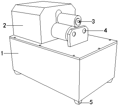
[0020] see figure 1 , the present invention provides a wafer dotting device, the structure of which includes: a body 1, a reaction box 2, a conveying roller 3, a power shaft 4, and a foot 5, the top of the body 1 is provided with a reaction box 2, and the reaction The side of the box body 2 is connected to the conveying roller 3 and the power shaft 4. The conveying roller 3 and the power shaft 4 are connected to each other and linked together. The feet 5 are located at the four corners of the bottom of the body 1. The whole body 1 is a rectangular parallelepiped structure, which is high-strength It is composed of metal plates and has a cavity inside which can be used to load other components of the equipment. On the one hand, it is used for the installation and connection of the load-carrying structure, providing assembly space for it, and on the other hand, it is used to provide protection for the components. The shell can protect the components. When receiving external impa...
PUM
 Abstract
Description
Claims
Application Information
 - R&D
- Intellectual Property
- Life Sciences
- Materials
- Tech Scout
- Unparalleled Data Quality
- Higher Quality Content
- 60% Fewer Hallucinations
Browse by: Latest US Patents, China's latest patents, Technical Efficacy Thesaurus, Application Domain, Technology Topic, Popular Technical Reports.
© 2025 PatSnap. All rights reserved.Legal|Privacy policy|Modern Slavery Act Transparency Statement|Sitemap|About US| Contact US: help@patsnap.com