Display device and manufacturing method thereof

A technology for a display device and a manufacturing method, which is applied in semiconductor/solid-state device manufacturing, electrical components, electric solid-state devices, etc., can solve problems such as uneven grounding potential of display circuit boards and touch circuit boards, damage to display panels, etc., to achieve The design is simple, the principle is clear, and the effect of improving safety

Active Publication Date: 2020-02-28
BOE TECH GRP CO LTD +1
View PDF8 Cites 1 Cited by
  • Summary
  • Abstract
  • Description
  • Claims
  • Application Information

AI Technical Summary

Problems solved by technology

[0002] The market share of AMOLED display devices is getting higher and higher. At present, in order to achieve a higher screen ratio, various brands have introduced notch, water drop, and in-screen perforated display designs; however, with the popularization of 5G technology in the future, the existing size It may not meet the needs of consumers, so large-screen display may become a direction of future development. Considering the portability of mobile communication devices and the excellent performance of AMOLED's flexibility and bendability, foldable screens are bound to receive wider attention in the future. Pay attention to
[0003]

Method used


Image

  • Display device and manufacturing method thereof
  • Display device and manufacturing method thereof
  • Display device and manufacturing method thereof

Examples


Example Embodiment

[0050] In order to make the technical solutions and advantages of the present invention clearer, the following further describes the embodiments of the present invention in detail with reference to the accompanying drawings.

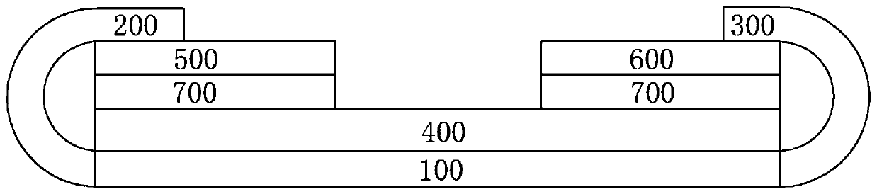
[0051] An embodiment of the present invention provides a display device, such as figure 2 As shown, the display device includes: a display panel 100, a display circuit board 200, a touch circuit board 300, a support layer 400, a first heat dissipation layer 500, and a second heat dissipation layer 600.

[0052] Specifically, in figure 2 In the example, the display panel 100 may be a touch display panel 100, wherein the first end of the display circuit board 200 is electrically connected to the display panel 100, the first end of the touch circuit board 300 is electrically connected to the display panel 100, and the support layer 400 is provided on the surface of the display panel 100, figure 2 In the example, an adhesive layer 700 is further provided on bot...


PUM


Abstract

The invention discloses a display device, which comprises a display panel, a display circuit board, a touch circuit board, a support layer, a first heat dissipation layer and a second heat dissipationlayer. A first end of the display circuit board is electrically connected to the display panel. A first end of the touch circuit board is electrically connected to the display panel. The support layer is disposed on the surface of the display panel. The first heat dissipation layer and the second heat dissipation layer are respectively arranged on both sides of the support layer. A second end ofthe display circuit board and a second end of the touch circuit board are respectively arranged on the first heat dissipation layer and the second heat dissipation layer. A connecting piece is also arranged between the first heat dissipation layer and the second heat dissipation layer. According to the invention, since the connecting piece is arranged between the first heat dissipation layer and the second heat dissipation lay, it is further ensured that electrical connection between the display circuit board and the touch circuit board is realized, so that the grounding potential between thedisplay circuit board and the touch circuit board is the same, the situation that the display panel is injured during electrostatic testing is avoided, and the safety is improved.

Description

Technical field [0001] The present invention relates to the field of display technology. More specifically, it relates to a display device and a manufacturing method Background technique [0002] The market share of AMOLED display devices is getting higher and higher. At present, in order to achieve a higher screen-to-body ratio, various brands have introduced bangs, water drops, and in-screen perforated display designs; however, with the popularization of 5G technology in the future, the existing size It may not meet the needs of consumers, so large-screen display may become a direction of future development. Considering the portability of mobile communication devices and the excellent performance of AMOLED with flexibility and bending, the future foldable screen is bound to be more widely used. Pay attention. [0003] figure 1 It shows a schematic diagram of the layer structure of an AMOLED display device in the prior art. In order to achieve foldability, the heat dissipation l...

Claims


Application Information

Patent Timeline
IPC IPC(8): H01L51/52H01L27/32H01L51/56
CPCH10K59/40H10K50/87H10K71/00H10K59/131H10K50/8426H10K59/1201
Inventor 陈栋杨亚馨
Owner BOE TECH GRP CO LTD
Why Eureka
Try Eureka