Inverted LED chip for backlight display and manufacturing method thereof
An LED chip and backlight display technology, applied in electrical components, circuits, semiconductor devices, etc., can solve problems such as increasing the thickness of the display screen, and achieve the effect of increasing the light output angle
- Summary
- Abstract
- Description
- Claims
- Application Information
AI Technical Summary
Problems solved by technology
Method used
Image

Examples
Embodiment Construction
[0032] In order to make the object, technical solution and advantages of the present invention clearer, the present invention will be further described in detail below in conjunction with the accompanying drawings.
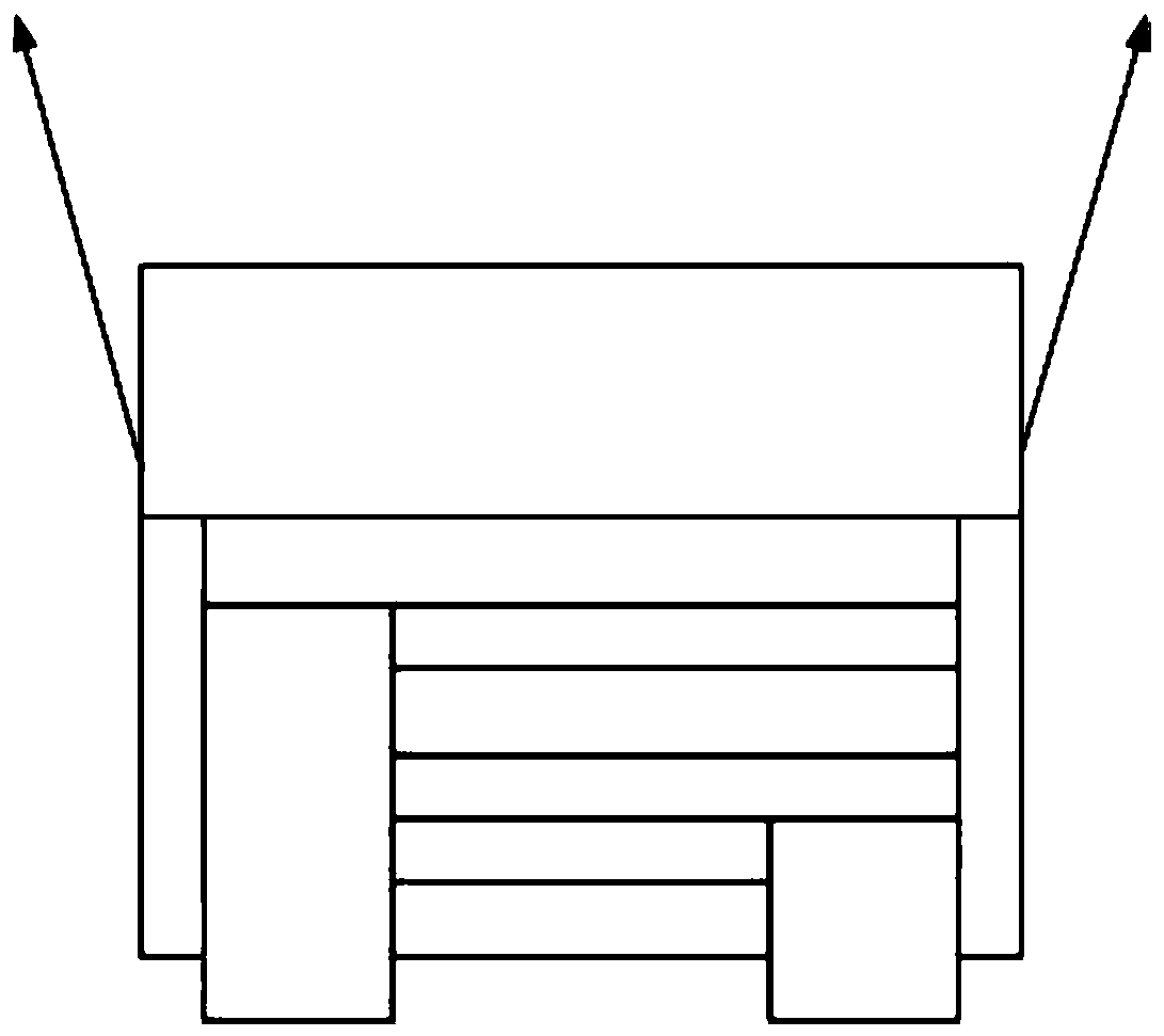
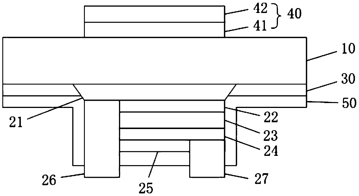
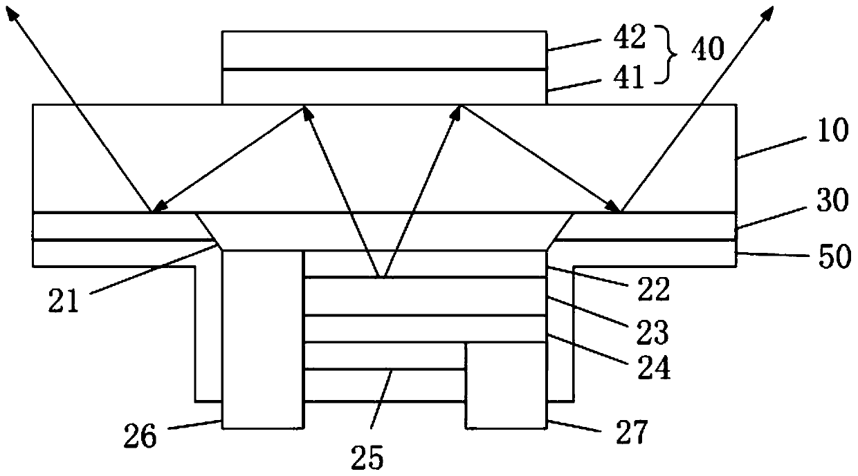
[0033] see figure 2 , a flip-chip LED chip for backlight display provided by the present invention includes a substrate 10 , a light-emitting structure, a first reflective layer 30 and a scattering layer 40 .
[0034] The front of the substrate 10 includes a light-emitting area and a reflective area, the reflective area is located around the light-emitting area, the back of the substrate 10 is provided with a scattering area and a light-emitting area, and the reflective area is located around the light-emitting area, so The light emitting area is located around the scattering area, and the scattering area is located above the light emitting area.
[0035] The light emitting structure of the present invention is set in the light emitting area, and the first refle...
PUM
| Property | Measurement | Unit |
|---|---|---|
| Thickness | aaaaa | aaaaa |
| Thickness | aaaaa | aaaaa |
Abstract
Description
Claims
Application Information
PatSnap Eureka turns technology decisions into work you can execute. Powered by our Innovation Knowledge Graph, it runs expert workflows across engineering, life sciences, materials and intellectual property. Get your review-ready output in minutes.


