Panel drive circuit

A panel drive circuit and drive signal technology, applied in the direction of instruments, static indicators, etc., can solve the problems of uneven surrounding brightness, complex circuit structure, difficult to achieve narrow borders of display panels, etc., and achieve the effect of reducing the difficulty of design

Pending Publication Date: 2020-03-31
FUJIAN HUAJIACAI CO LTD
View PDF0 Cites 0 Cited by
  • Summary
  • Abstract
  • Description
  • Claims
  • Application Information

AI Technical Summary

Problems solved by technology

like Picture 1-1 As shown, the existing 7T2C circuit structure is relatively complex, and narrow borders are limited in panel design
Moreover, as the frame becomes smaller, the distance between the frame sealant and the active area (Active Area) in the display panel is closer, and the components in the active area are more likely to be polluted, resulting in problems such as uneven brightness around the area (Mura). It is difficult to realize the requirement of narrow frame of display panel

Method used


Image

  • Panel drive circuit
  • Panel drive circuit
  • Panel drive circuit

Examples


Embodiment Construction

[0016] In order to explain in detail the technical content, structural features, achieved goals and effects of the technical solution, the following will be described in detail in conjunction with specific embodiments and accompanying drawings.

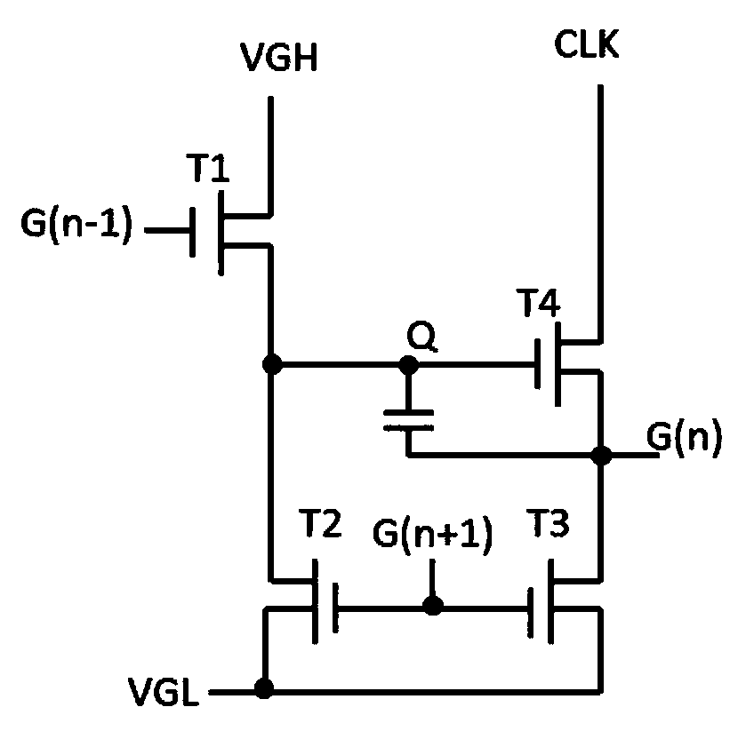
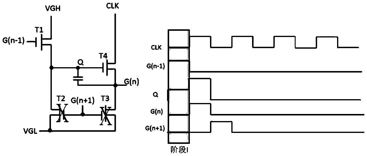
[0017] figure 1 It is a panel drive circuit of the present invention, including switch tubes T1, T2, T3, T4, and capacitors. The gate of T1 is connected to the upper-level drive signal, and the drain is connected to the gate of T4, one end of the capacitor, and T2 The source of T4 is connected to the other end of the capacitor and the source of T3, and the drain of T4 is also connected to the current level drive signal; the gates of T2 and T3 are connected to the next level drive signal , the drain of T2 is connected to the drain of T3. T1 is used as a pull-up TFT for pulling up the Q voltage to a high level; T2 is used as a pull-down TFT for pulling the Q point down to a low level. CLK signal and G(n-1), G(n), G(n+1) waveform sign...


PUM


Abstract

A panel drive circuit comprises switch tubes T1, T2, T3 and T4 and a capacitor, a grid electrode of the T1 is connected with an upper-stage driving signal, and a drain electrode of the T1 is connectedwith a grid electrode of the T4, one end of the capacitor and a source electrode of the T2; the drain electrode of the T4 is connected with the other end of the capacitor and the source electrode ofthe T3; the drain electrode of the T4 is also connected with a current-stage driving signal; and the grid electrodes of the T2 and the T3 are connected with a next-stage driving signal, and the drainelectrode of the T2 is connected with the drain electrode of the T3. By reducing the number of TFTs, the requirement of a narrow frame of the panel is met, and the design difficulty is reduced.

Description

technical field [0001] The invention relates to a new circuit design for reducing the space occupied by GIP. Background technique [0002] GIP technology (Gate Driver In Panel): array gate drive technology, widely used in liquid crystal display panels (LCD) and AMOLED display panels. The GIP technology is to fabricate the driving circuit of the horizontal scanning line on the substrate around the display area (Active Area), so that it can replace an external integrated circuit board (Integrated Circuit, IC) to complete the driving of the horizontal scanning line. The GIP technology can reduce the welding (bonding) process of the external IC and reduce the production cost. At present, the panel design mostly adopts double-sided GIP drivers to meet the requirements of display panels with narrow borders. Such as Picture 1-1 As shown, the existing 7T2C circuit structure is relatively complex, and the narrow frame is limited in the panel design. Moreover, as the frame becomes...

Claims


Application Information

Patent Timeline
Patent Type & Authority Applications(China)
IPC IPC(8): G09G3/36G09G3/3266G09G3/3225
CPCG09G3/3225G09G3/3266G09G3/3677
Inventor 罗敬凯
Owner FUJIAN HUAJIACAI CO LTD
Why Eureka
Try Eureka