A flat piezoelectric layer structure and manufacturing process of a bulk acoustic wave resonator

A bulk acoustic wave resonator and manufacturing process technology, applied in electrical components, impedance networks, etc., can solve problems such as filter bandwidth changes, device performance differences, cracking, etc.

Active Publication Date: 2021-11-19
HANGZHOU JWL TECH INC
View PDF4 Cites 0 Cited by
  • Summary
  • Abstract
  • Description
  • Claims
  • Application Information

AI Technical Summary

Problems solved by technology

[0006] As mentioned above, the film layer in the resonant area of ​​the bulk acoustic wave resonator is easily affected by external or self-stress, which may cause defects such as cracking, tympanic membrane, collapsed membrane, and bending. The stress change of the piezoelectric layer will cause the electromechanical coupling coefficient of the piezoelectric layer The change of the resonator will change the bandwidth of the filter composed of the resonator, which will lead to the difference in the performance of the device and affect the performance of the resonator.

Method used


Image

  • A flat piezoelectric layer structure and manufacturing process of a bulk acoustic wave resonator
  • A flat piezoelectric layer structure and manufacturing process of a bulk acoustic wave resonator
  • A flat piezoelectric layer structure and manufacturing process of a bulk acoustic wave resonator

Examples


Embodiment Construction

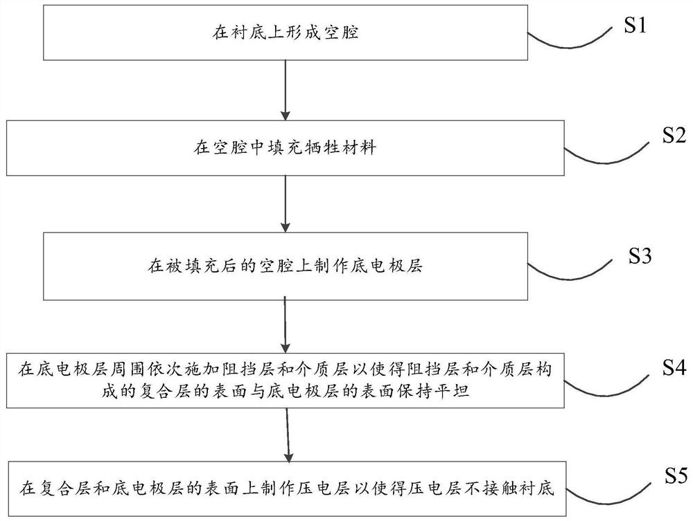
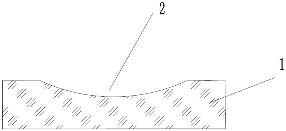
[0043] The application will be further described in detail below in conjunction with the accompanying drawings and embodiments. It should be understood that the specific embodiments described here are only used to explain related inventions, rather than to limit the invention. It should also be noted that, for the convenience of description, only the parts related to the related invention are shown in the drawings. It should be noted that the dimensions and sizes of components in the drawings are not to scale, and the size of some components may be highlighted for the sake of clarity.

[0044] It should be noted that, in the case of no conflict, the embodiments in the present application and the features in the embodiments can be combined with each other. The present application will be described in detail below with reference to the accompanying drawings and embodiments.

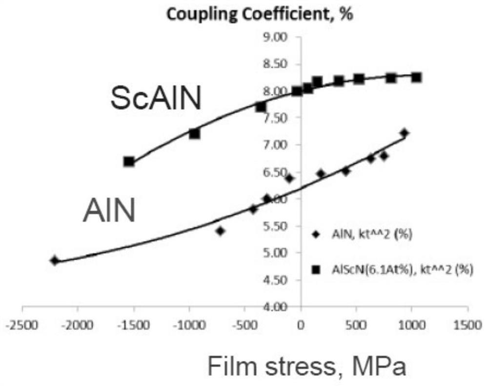
[0045] Such as figure 1 As shown, the stress change of the piezoelectric layer material will lead to ...


PUM

PropertyMeasurementUnit
thicknessaaaaaaaaaa

Abstract

The invention discloses a flat piezoelectric layer structure and a manufacturing process of a bulk acoustic wave resonator. A cavity is formed on a substrate; a sacrificial material is filled in the cavity; a bottom electrode layer is made on the filled cavity; A barrier layer and a dielectric layer are sequentially applied around the bottom electrode layer to keep the surface of the composite layer composed of the barrier layer and the dielectric layer flat with the surface of the bottom electrode layer; and a piezoelectric layer is formed on the surfaces of the composite layer and the bottom electrode layer to so that the piezoelectric layer does not contact the substrate. Improve the stress consistency of the piezoelectric layer, reduce the stress effect of the piezoelectric layer, control the electromechanical coupling coefficient of the device in the optimal range, improve the quality factor of the resonator, the device yield and the consistency and reliability of the device finished product, and Device size can be reduced by making the effective resonant area larger and closer to but not beyond the cavity. By arranging the seed layer and the passivation layer, the bottom electrode layer and the top electrode layer can be protected, and the bottom electrode layer can be fabricated inside the resonator to maintain mechanical stability.

Description

technical field [0001] This application relates to the field of communication devices, and mainly relates to a flat piezoelectric layer structure and manufacturing process of a bulk acoustic wave resonator. Background technique [0002] With the increasingly crowded electromagnetic spectrum and the increase of frequency bands and functions of wireless communication equipment, the electromagnetic spectrum used by wireless communication has grown rapidly from 500MHz to above 5GHz, and it is also necessary for the RF front-end module with high performance, low cost, low power consumption and small size. The demand is increasing day by day. The filter is one of the RF front-end modules, which can improve the transmitted and received signals, and is mainly composed of multiple resonators connected through a topology network structure. Fbar (Thin film bulk acoustic resonator) is a bulk acoustic resonator. The filter composed of it has the advantages of small size, strong integrat...

Claims


Application Information

Patent Timeline
Patent Type & Authority Patents(China)
IPC IPC(8): H03H3/02
CPCH03H3/02H03H2003/027
Inventor 李林萍盛荆浩江舟
Owner HANGZHOU JWL TECH INC
Why Eureka
Try Eureka