Thin film resonator and method for manufacturing the same

a resonator and film technology, applied in piezoelectric/electrostrictive/magnetostrictive devices, piezoelectric/electrostriction/magnetostriction machines, semiconductor devices, etc., can solve the problems of large insertion loss below 3 db, mmic, and insufficient size of smd resonators, etc., to achieve high integration onto the substrate, reduce manufacturing costs, and increase yield

Inactive Publication Date: 2003-02-13
MEMS SOLUTIONS INC
View PDF3 Cites 45 Cited by
  • Summary
  • Abstract
  • Description
  • Claims
  • Application Information

AI Technical Summary

Benefits of technology

0049] According to the present invention, the thin film resonator is manufactured using MEMS technology without etching the substrate to have minute dimensions below hundreds of micrometers. Hence, the thin film resonator is exceptionally small and can be highly integrated onto the substrate. Also, the thickness of the dielectric layer of the thin film resonator can be adjusted to achieve the integration of multiple bands including radio frequency (RF), intermediate frequency (IF) and low frequency (LF) by controlling the thickness of the dielectric layer. Also, an inductor and a capacitor can be integrated.
0050] In addition, yields can be increased and manufacturing costs can be greatly reduced since the thin film resonator can be manufactured without etching or machining the silicon substrate. Therefore, the manufacturing process of the present invention has excellent advantages during mass production, including simplicity and ease of packaging. Also, the thin film resonator of the present invention has a good quality factor of about 1000 to 10000 and a low insertion loss of under 2 dB, because the thin film resonator has minute patterns and a three-dimensional, floating construction, and is easily manufactured using the MEMS technology.
0051] Furthermore, the thin film resonator of the present invention can minimize any interference due to its substrate, and has ideal dimensions because of its compact substrate, making the thin film resonator exceptionally small yet comprising three-dimensional, floating construction.

Problems solved by technology

However, the dielectric filter is too large to be applied in a monolithic microwave integrated circuit (MMIC).
Though the mono-blocked or the multi-layered surface mounted device (SMD) resonators are now developed with smaller dimensions, SMD resonators do not sufficiently overcome their size problems.
However, the SAW filter has large insertion losses below 3 dB and its manufacturing costs are high because it is manufactured using single crystal I5 piezoelectric substrate composed of lithium niobate (LiNbO.sub.3) or lithium titanate (LiTaO.sub.3).
However, passive components of RF technology such as the filter, the duplexer filter or the antenna are relatively large and complicated structures so that the single chip may not be achieved due to passive components.
Hence, the conventional FBAR provides poor quality performance with an increased insertion loss.
In addition, the interference of the substrate may not be blocked, causing the power loss of the FBAR to increase.
Furthermore, the process for etching the silicon substrate demands much time, and the cost of manufacturing the FBAR increases because the conventional FBAR is formed on the silicon substrate where the cavity is positioned.
However, the TFBAR may not be mass-produced and packaging the TFBAR may be difficult since its structure is complicated and the integration device including the TFBAR is difficult.

Method used


Image

  • Thin film resonator and method for manufacturing the same
  • Thin film resonator and method for manufacturing the same
  • Thin film resonator and method for manufacturing the same

Examples


Embodiment Construction

[0058] Hereinafter, preferred embodiments of the present invention will be described in more detail with reference to the accompanying drawings, but it is understood that the present invention should not be limited to the following embodiments.

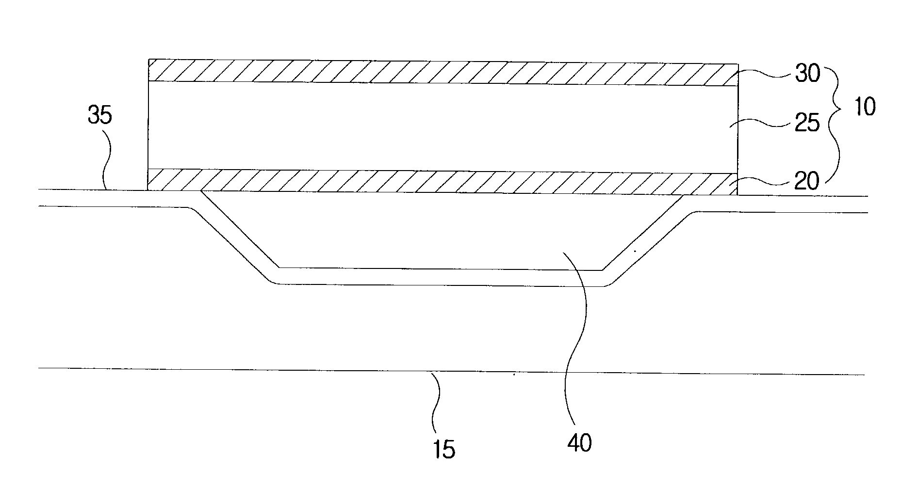
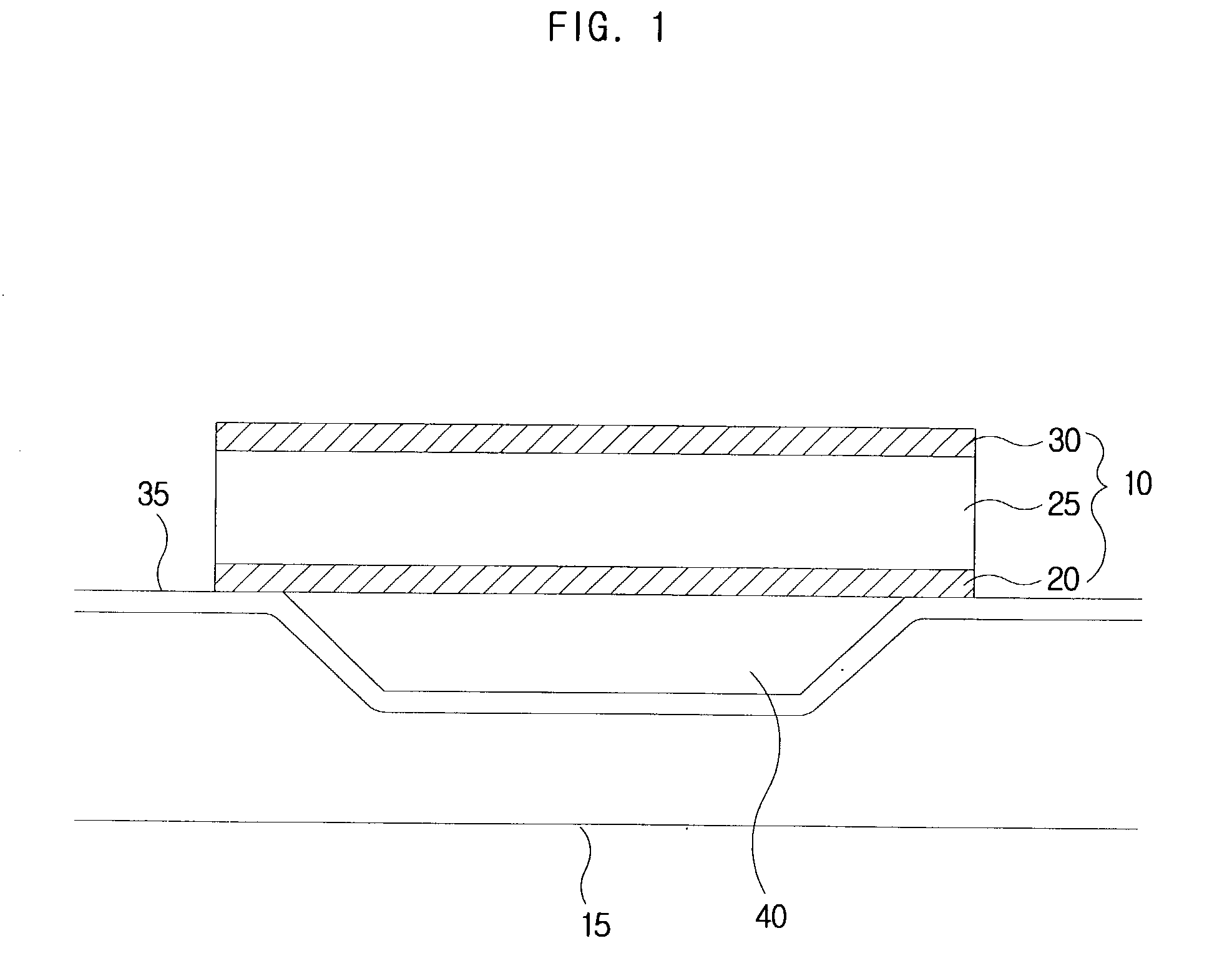
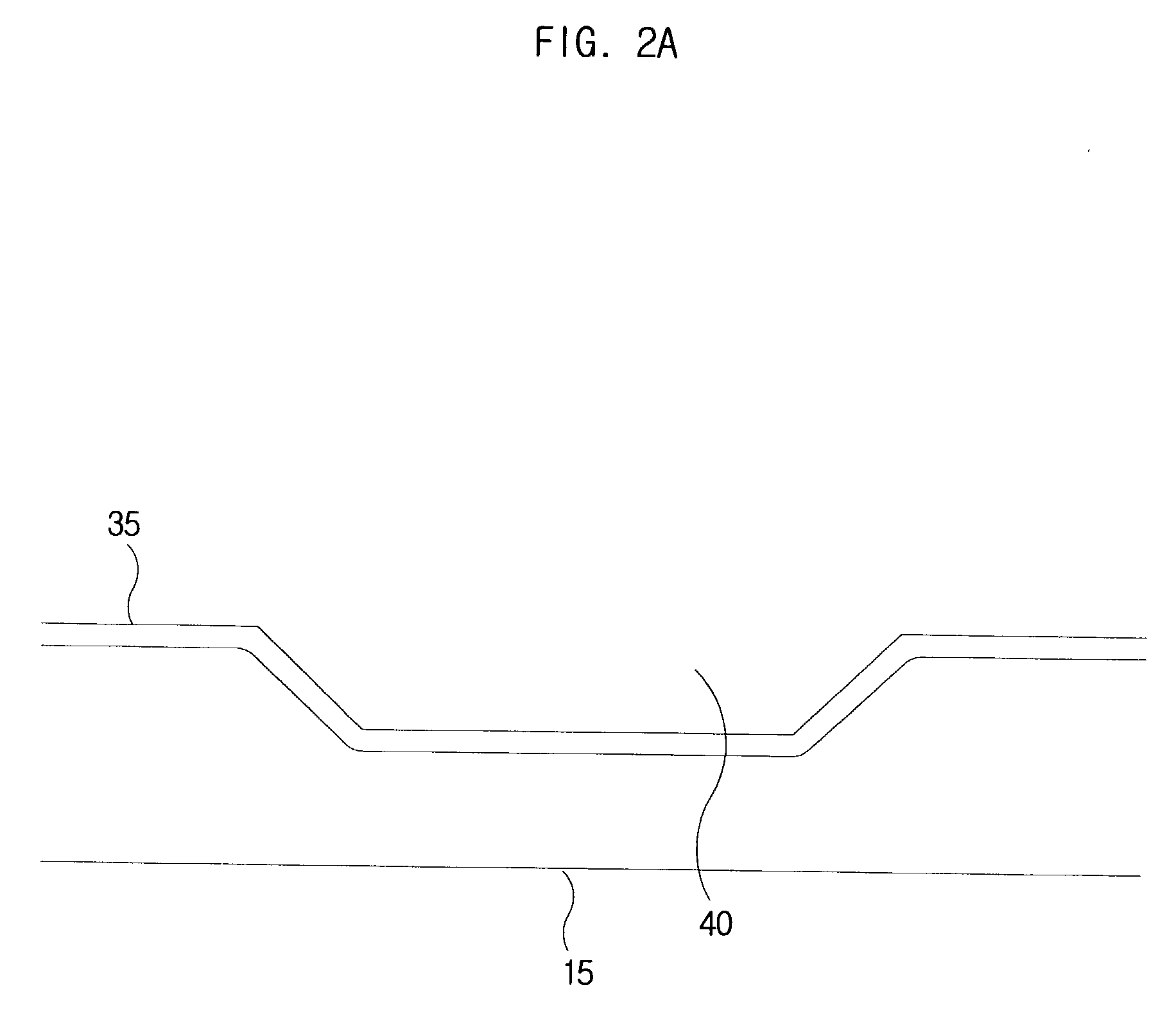
[0059] FIG. 3 is a perspective view showing a thin film resonator according to one preferred embodiment of the present invention and FIG. 4 is a cross-sectional view showing the thin film resonator in FIG. 3.

[0060] Referring to FIGS. 3 and 4, a thin film resonator 100 according to the present invention has a supporting member 190, a first electrode 165, a dielectric layer 175 and a second electrode 185. The thin film resonator 100 is formed on a substrate 110 and a first air gap 200 is interposed between the thin film resonator 100 and the substrate 110.

[0061] The supporting member 190 supports the thin film resonator 100 and includes a supporting layer 155 and a plurality of posts 140 and 141. The supporting layer 155 is composed of silicon n...


PUM

PropertyMeasurementUnit
temperaturesaaaaaaaaaa
insertion lossesaaaaaaaaaa

Abstract

A thin film resonator having enhanced performance and a manufacturing method thereof are disclosed. The thin film resonator includes a supporting means, a first electrode, a dielectric layer and a second electrode. The supporting means has several posts and a supporting layer formed on the posts. The first electrode, the dielectric layer and the second electrode are successively formed on the supporting layer. The thin film resonator is exceptionally small and can be highly integrated, and the thickness of the dielectric layer of the resonator can be adjusted to achieve the integration of multiple bands including radio, intermediate and low frequencies. Also, the thin film resonator can minimize interference and has ideal dimensions because of its compact substrate, making the thin film resonator exceptionally small, yet comprising a three-dimensional, floating construction.

Description

[0001] The present invention relates to a thin film resonator and a method for manufacturing the same, and more particularly to an integrated thin film resonator with multiple bands to enhance performance and an easy method for manufacturing the same.[0002] Mobile communications has been rapidly developed as the main instrument serving the information society. This instrument has been influenced by the developments of two technologies: signal processing using modulation or demodulation of transmitted data over limited frequency bands, and the technology of manufacturing radio frequency (RF) hardware parts.[0003] In particular, filters are most important among the parts used for RF mobile communication devices. Filters are able to select the signal requested by the user from numerous signals on the public communication network, or filter a signal transferred by the user. Thus, excellent filters were previously developed for high quality mobile communication. Recently, higher performa...

Claims


Application Information

Patent Timeline
Patent Type & Authority Applications(United States)
IPC IPC(8): H03H9/00H03H3/02H03H3/04H03H9/05H03H9/10H03H9/13H03H9/17
CPCH03H3/04H03H9/02133H03H9/0542H03H9/172H03H2003/027H03H2009/241H03H9/00
Inventor KIM, EON-KYEONG
Owner MEMS SOLUTIONS INC
Why Eureka
Try Eureka