Flat piezoelectric layer structure of bulk acoustic wave resonator and manufacturing process

A bulk acoustic wave resonator and manufacturing process technology, applied in electrical components, impedance networks, etc., can solve problems such as cracking, affecting the performance of the resonator, and changing the filter bandwidth.

Active Publication Date: 2020-05-15
HANGZHOU JWL TECH INC
View PDF8 Cites 15 Cited by
  • Summary
  • Abstract
  • Description
  • Claims
  • Application Information

AI Technical Summary

Problems solved by technology

[0006] As mentioned above, the film layer in the resonant area of ​​the bulk acoustic wave resonator is easily affected by external or self-stress, which may cause defects such as cracking, tympanic membrane, collapsed membrane, and bending. The stress change of the piezoelectric lay...

Method used


Image

  • Flat piezoelectric layer structure of bulk acoustic wave resonator and manufacturing process
  • Flat piezoelectric layer structure of bulk acoustic wave resonator and manufacturing process
  • Flat piezoelectric layer structure of bulk acoustic wave resonator and manufacturing process

Examples


Embodiment Construction

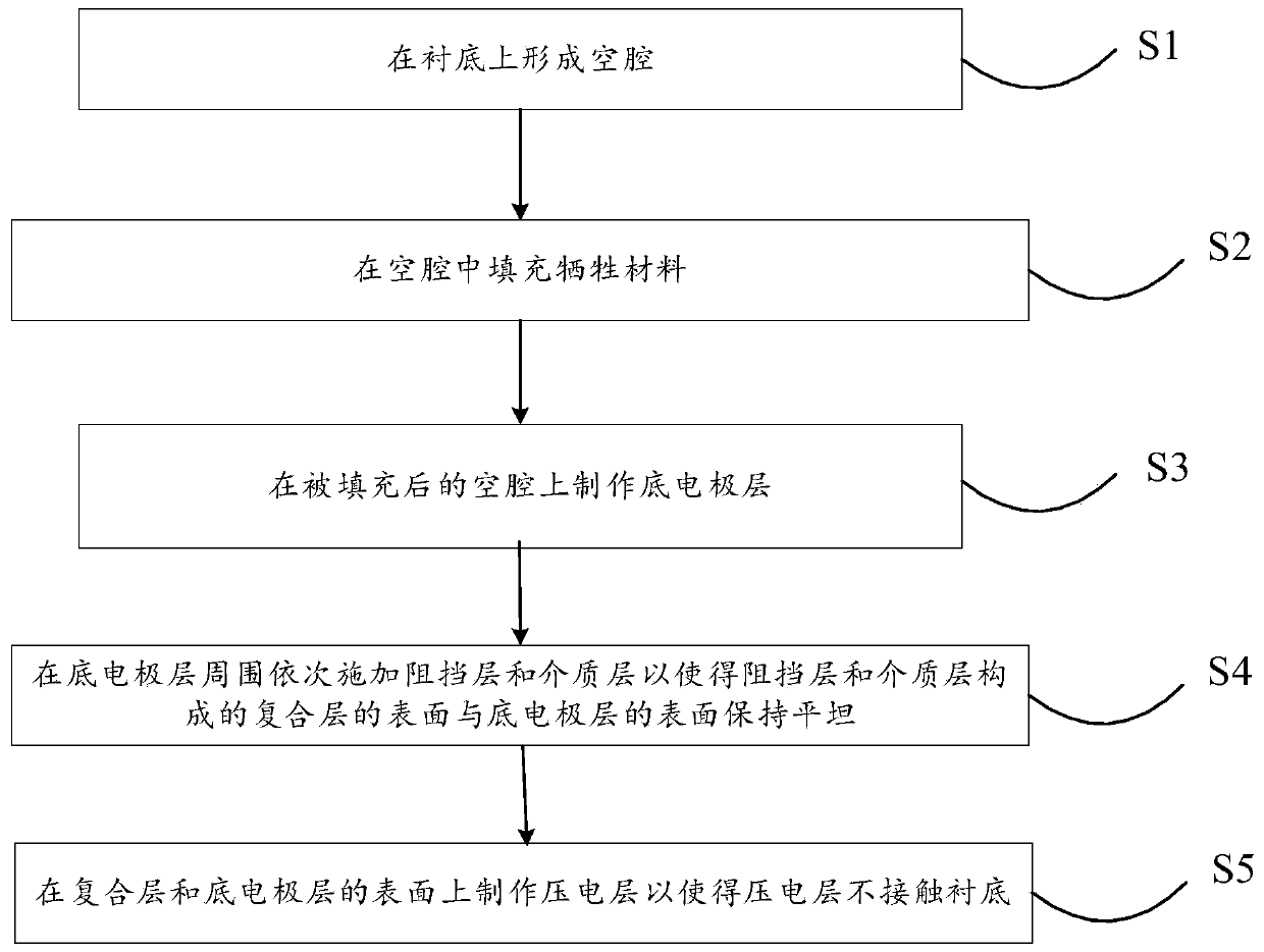
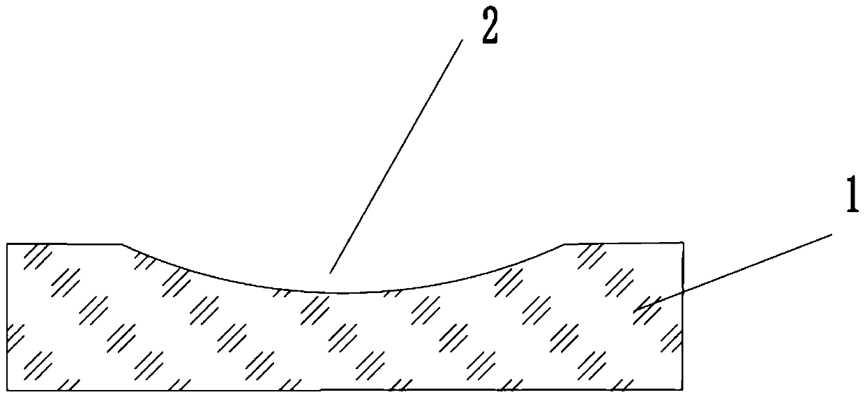
[0043] The application will be further described in detail below with reference to the drawings and embodiments. It can be understood that the specific embodiments described here are only used to explain the related invention, but not to limit the invention. In addition, it should be noted that, for ease of description, only the parts related to the relevant invention are shown in the drawings. It should be noted that the dimensions and sizes of the components in the drawings are not to scale, and the sizes of some components may be highlighted for obvious reasons.

[0044] It should be noted that the embodiments in the application and the features in the embodiments can be combined with each other if there is no conflict. Hereinafter, the present application will be described in detail with reference to the drawings and in conjunction with embodiments.

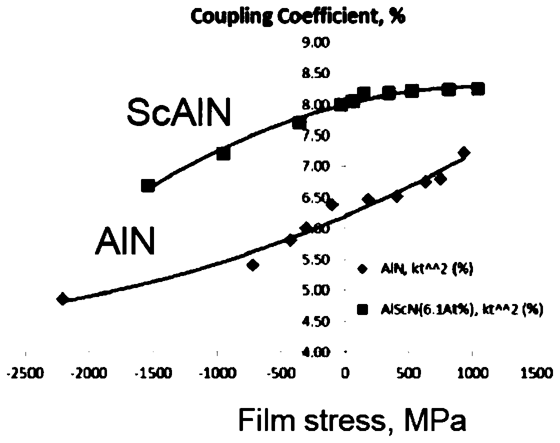
[0045] Such as figure 1 As shown, the stress change of the piezoelectric layer material will cause the change of the electrome...


PUM

PropertyMeasurementUnit
Thicknessaaaaaaaaaa

Abstract

The invention discloses a flat piezoelectric layer structure of a bulk acoustic wave resonator and a manufacturing process. The manufacturing process comprises the following steps: forming a cavity ona substrate; filling a sacrificial material in the cavity; manufacturing a bottom electrode layer on the filled cavity; sequentially applying a barrier layer and a dielectric layer around the bottomelectrode layer to keep the surface of a composite layer formed by the barrier layer and the dielectric layer flat with the surface of the bottom electrode layer; and fabricating a piezoelectric layeron the surfaces of the composite layer and the bottom electrode layer so that the piezoelectric layer does not contact the substrate. The stress consistency of the piezoelectric layer is improved, the stress influence of the piezoelectric layer is reduced, an electromechanical coupling coefficient of a device is controlled within the optimal range, the quality factor of the resonator, the yield of the device and the consistency and reliability of the finished product of the device are improved, the effective resonance area is larger and closer to the cavity and does not exceed the cavity, andthe size of the device can be reduced. By arranging a seed layer and a passivation layer, the bottom electrode layer and the top electrode layer can be protected, the bottom electrode layer is manufactured inside the resonator, and the mechanical stability is maintained.

Description

Technical field [0001] The application relates to the field of communication devices, and mainly relates to a flat piezoelectric layer structure and manufacturing process of a bulk acoustic wave resonator. Background technique [0002] With the increasing congestion of the electromagnetic spectrum and the increase in the frequency bands and functions of wireless communication equipment, the electromagnetic spectrum used in wireless communication has grown rapidly from 500MHz to above 5GHz. It is also important for the high performance, low cost, low power consumption, and small size of the RF front-end module. The demand is increasing. The filter is one of the RF front-end modules, which can improve the transmission and reception of the signal. It is mainly composed of multiple resonators connected through a topological network structure. Fbar (Thin film bulk acoustic resonator) is a bulk acoustic wave resonator. The filter composed of it has the advantages of small size, strong...

Claims


Application Information

Patent Timeline
IPC IPC(8): H03H3/02
CPCH03H3/02H03H2003/027
Inventor 李林萍盛荆浩江舟
Owner HANGZHOU JWL TECH INC
Why Eureka
Try Eureka