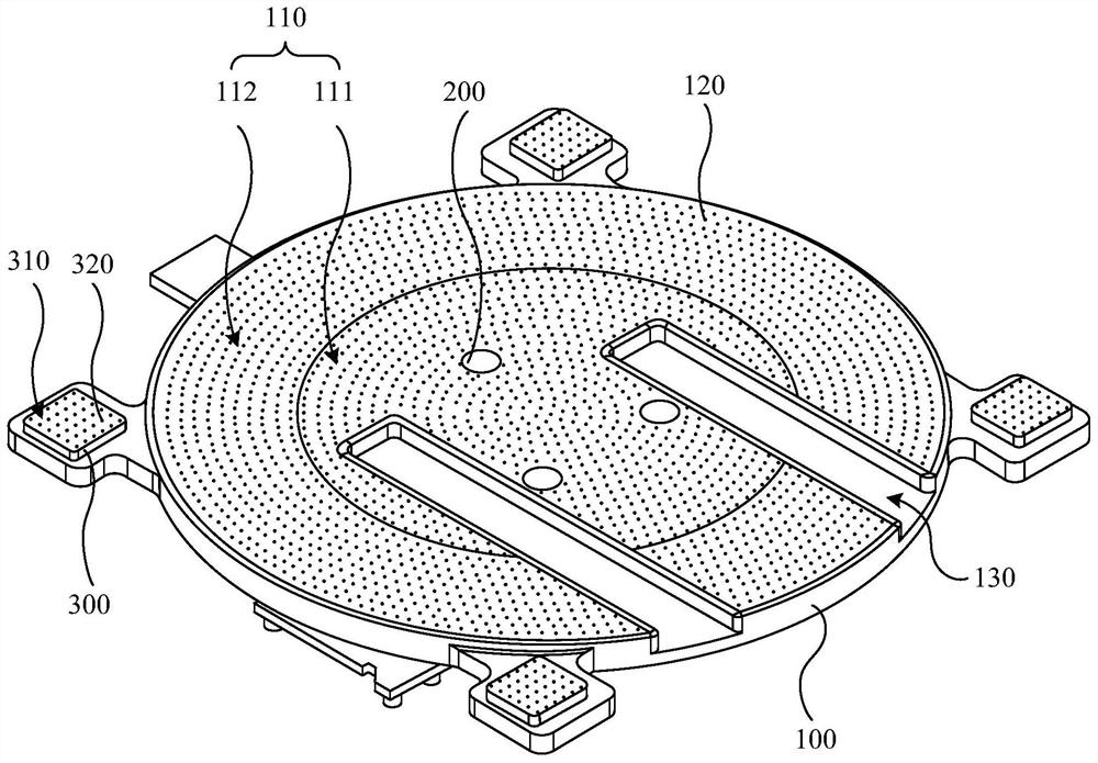
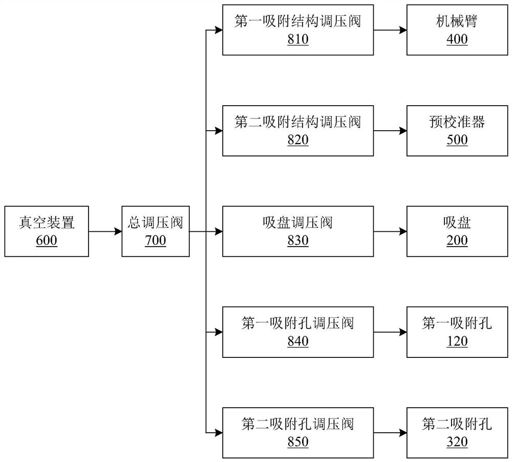
wafer carrier
A wafer carrying and vacuum device technology, which is applied in the manufacture of electrical components, circuits, semiconductor/solid-state devices, etc., can solve problems such as large bow value of the wafer, uneven wafer surface, adverse effects of semiconductor device manufacturing and testing, etc. , to achieve the effect of reducing the bow value
- Summary
- Abstract
- Description
- Claims
- Application Information
AI Technical Summary
Problems solved by technology
Method used
Image

Examples
Embodiment Construction
[0019] The present invention will be described in more detail below with reference to the accompanying drawings. In the various figures, like elements are designated by like reference numerals. For the sake of clarity, various parts in the figures have not been drawn to scale. Additionally, some well-known parts may not be shown in the drawings.
[0020] Numerous specific details of the invention are described below, such as the construction of components, materials, dimensions, processing and techniques, in order to provide a clearer understanding of the invention. However, as can be understood by one skilled in the art, the present invention may be practiced without these specific details.
[0021] It will be understood that, in describing the structure of a component, when a layer or region is referred to as being "on" or "over" another layer or region, it can be directly on the other layer or region, or Other layers or regions are also included between it and another la...
PUM
 Abstract
Description
Claims
Application Information
 - R&D Engineer
- R&D Manager
- IP Professional
- Industry Leading Data Capabilities
- Powerful AI technology
- Patent DNA Extraction
Browse by: Latest US Patents, China's latest patents, Technical Efficacy Thesaurus, Application Domain, Technology Topic.
© 2024 PatSnap. All rights reserved.Legal|Privacy policy|Modern Slavery Act Transparency Statement|Sitemap