Photosensitive thin film transistor, display panel and display device

A technology of thin film transistors and display panels, which is applied in the direction of electric solid-state devices, semiconductor devices, electrical components, etc., and can solve problems such as inability to carry out signals, small capacitance signal volume, and reading

Active Publication Date: 2020-06-05
YUNGU GUAN TECH CO LTD
View PDF6 Cites 5 Cited by
  • Summary
  • Abstract
  • Description
  • Claims
  • Application Information

AI Technical Summary

Problems solved by technology

There are mainly three ways to realize fingerprint identification: capacitive, optical and ultrasonic. Capacitive generally has the problem that the capacitance signal is very small when the distance between the finger and the sensor electrode is more than 300um, and the signal cannot be read. Due to the excessive media in the display area of ​​the ultrasonic type, there are still technical security issues. Optical fingerprint recognition is a better fingerprint recognition method integrated in the displa...

Method used


Image

  • Photosensitive thin film transistor, display panel and display device
  • Photosensitive thin film transistor, display panel and display device
  • Photosensitive thin film transistor, display panel and display device

Examples


Embodiment Construction

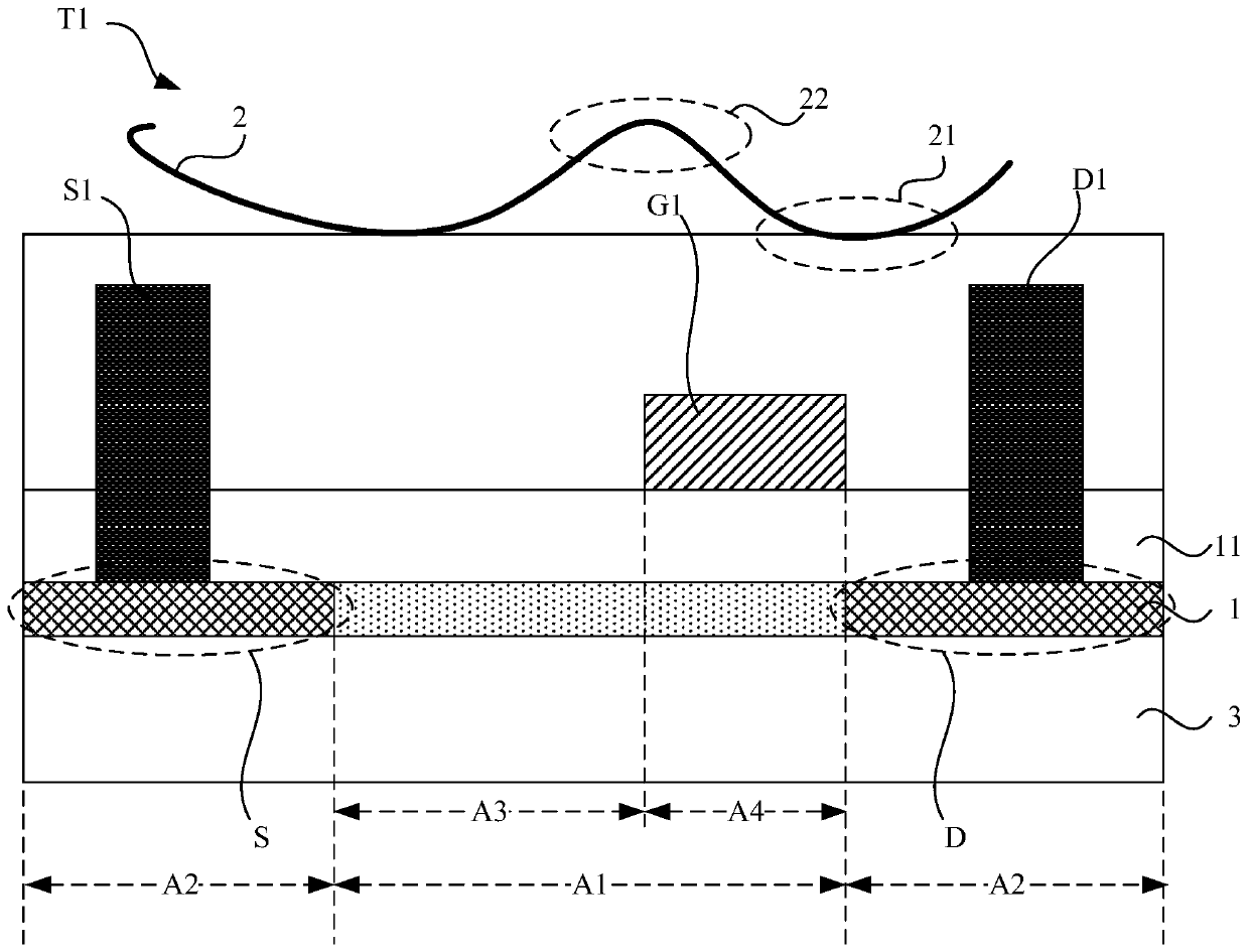
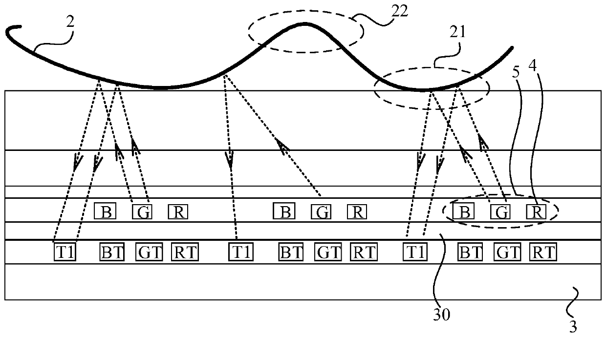
[0030] The present invention will be further described in detail below in conjunction with the accompanying drawings and embodiments. It should be understood that the specific embodiments described here are only used to explain the present invention, but not to limit the present invention. In addition, it should be noted that, for the convenience of description, only some structures related to the present invention are shown in the drawings but not all structures.

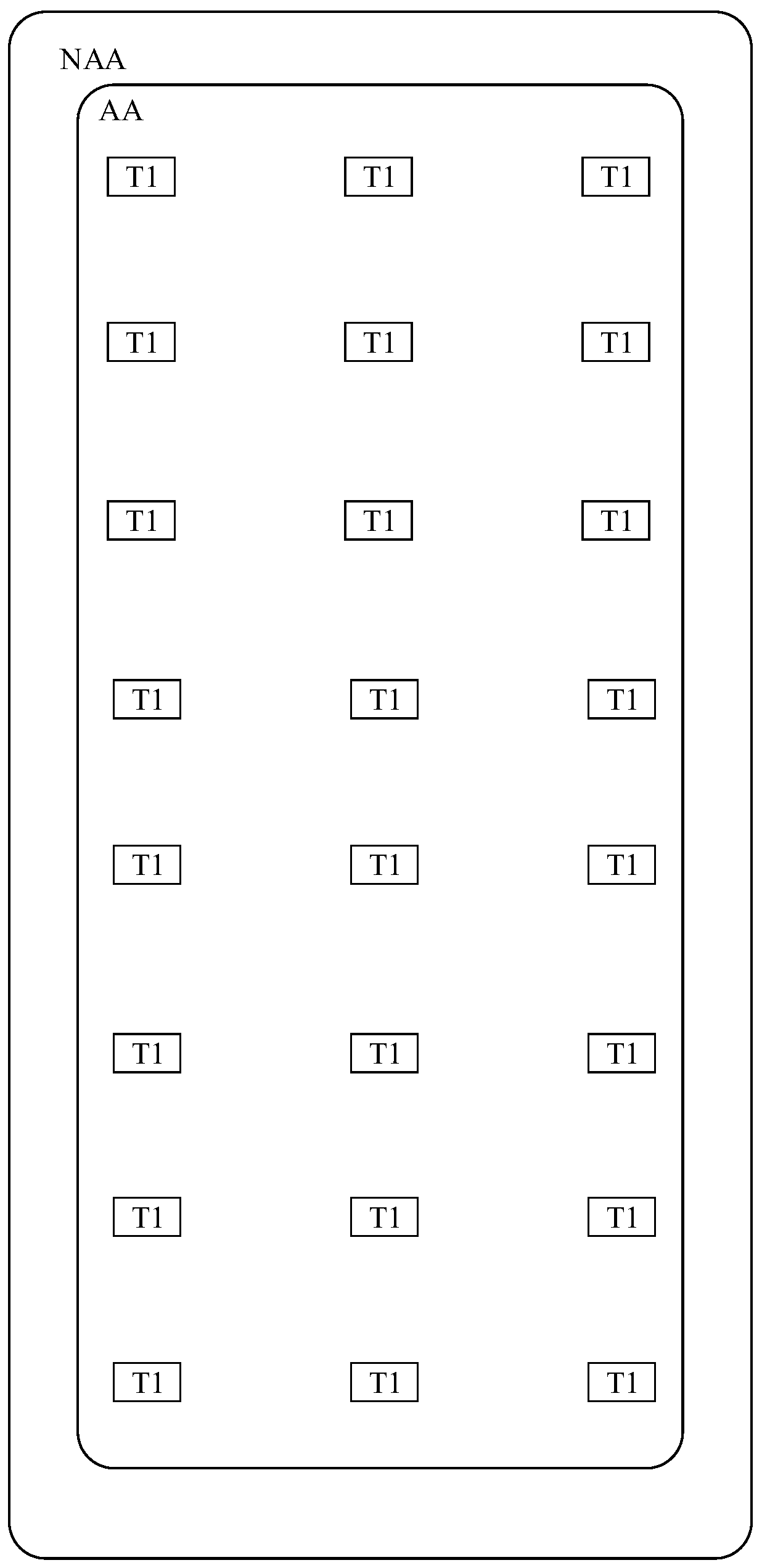
[0031] As mentioned in the background technology, the existing optical fingerprint recognition is generally a fixed-position fingerprint recognition, that is, the fingerprint recognition sensor is fixed at a certain position in the screen body. The pass rate is specially designed, such as increasing the light transmittance at this position, and placing a fingerprint recognition sensor under the screen at this position. With the development of fingerprint identification technology, how to realize large-area or even...


PUM


Abstract

The embodiment of the invention discloses a photosensitive thin film transistor, a display panel and a display device. The photosensitive thin film transistor comprises: an active layer, wherein the active layer comprises a first doped region and second doped regions located on the two sides of the first doped region, the doping concentration of the second doped regions is larger than that of thefirst doped region, and the two second doped regions correspondingly form a source electrode and a drain electrode of the light-sensitive thin film transistor; and a grid electrode, wherein the grid electrode is located above the active layer, the area of the grid electrode is smaller than that of the first doped region, the vertical projection of the first doped region covers the vertical projection of the grid electrode, and the part, not shielded by the grid electrode, of the first doped region is used for adjusting photo-generated current generated by the photosensitive thin film transistor according to light reflected to the first doped region through the touch body. Through the technical scheme provided by the embodiment of the invention, fingerprint identification can be realized ina large-area range or even a full-screen range of the display panel.

Description

technical field [0001] Embodiments of the present invention relate to the field of display technology, and in particular to a photosensitive thin film transistor, a display panel and a display device. Background technique [0002] Fingerprint identification refers to identity identification by comparing the detailed feature points of different fingerprints. Each person's fingerprints are different, even the fingerprints of the same person's ten fingers are also significantly different, so fingerprints can be used for identity identification. There are mainly three ways to realize fingerprint identification: capacitive, optical and ultrasonic. Capacitive generally has the problem that the capacitance signal is very small when the distance between the finger and the sensor electrode is more than 300um, and the signal cannot be read. Due to the excessive media in the display area of ​​the ultrasonic type, there are still technical security problems. Optical fingerprint recognit...

Claims


Application Information

Patent Timeline
IPC IPC(8): H01L31/0224H01L31/0352H01L31/113H01L27/32
CPCH01L31/1136H01L31/0352H01L31/022408H10K59/00H10K59/12
Inventor 胡祖权孙增标
Owner YUNGU GUAN TECH CO LTD
Why Eureka
Try Eureka