Packaging structure and packaging method of chip

A packaging method and packaging structure technology, which is applied in the manufacture of electrical components, electrical solid devices, semiconductor/solid devices, etc., can solve the problems of difficult control of the dispensing process and high development costs

Active Publication Date: 2020-07-07
QINGDAO GOERTEK INTELLIGENT SENSOR CO LTD
View PDF3 Cites 5 Cited by
  • Summary
  • Abstract
  • Description
  • Claims
  • Application Information

AI Technical Summary

Problems solved by technology

[0004] The main purpose of the present invention is to provide a chip packaging structure and packaging method, which aims to improve the current part of the exposed

Method used


Image

  • Packaging structure and packaging method of chip
  • Packaging structure and packaging method of chip
  • Packaging structure and packaging method of chip

Examples


Example Embodiment

[0038] The technical solutions in the embodiments of the present invention will be clearly and completely described below. Obviously, the described embodiments are only a part of the embodiments of the present invention, rather than all the embodiments. Based on the embodiments of the present invention, all other embodiments obtained by those of ordinary skill in the art without creative work shall fall within the protection scope of the present invention.

[0039] In addition, the technical solutions between the various embodiments of the present invention can be combined with each other, but they must be based on what can be achieved by those of ordinary skill in the art. When the combination of technical solutions is contradictory or cannot be achieved, it should be considered that the combination of such technical solutions It does not exist and does not fall within the scope of protection claimed by the present invention.

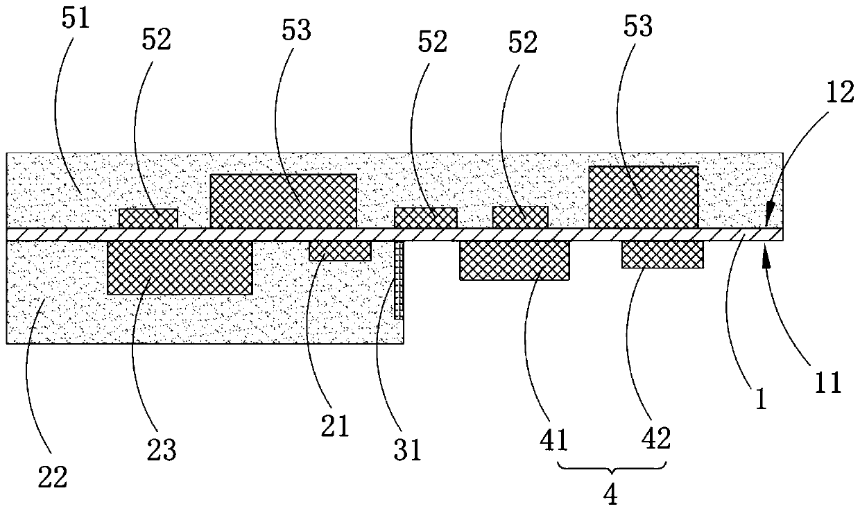
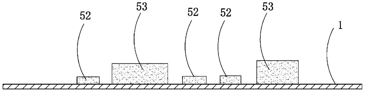
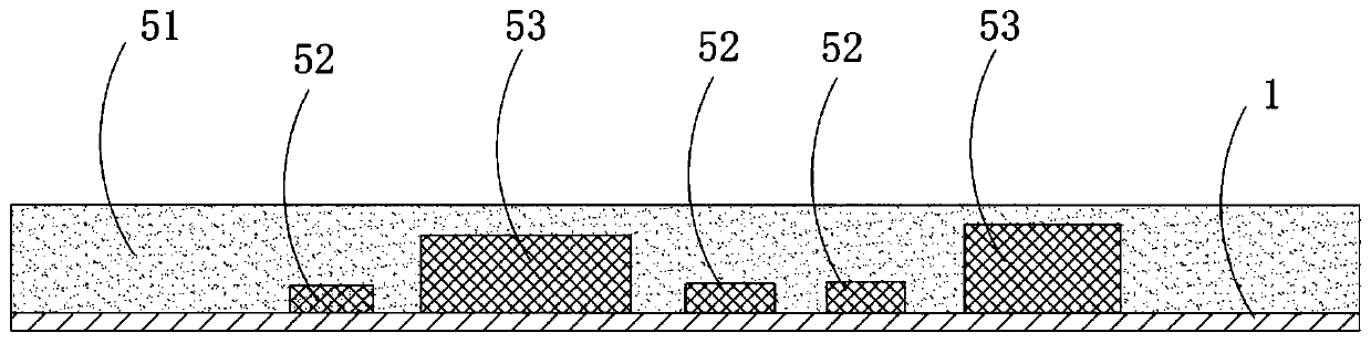
[0040] In addition, the present invention provides a ...


PUM


Abstract

The invention discloses a chip packaging structure and method, and the method comprises the following steps: installing a first chip and a first element assembly on a first surface of a substrate; installing a cover body structure on the first surface to enable the cover body structure to cover the first element assembly; carrying out plastic package on the first surface of the substrate to form afirst pre-plastic package layer, the first chip and the cover body structure being located in the first pre-plastic package layer; and cutting the first pre-plastic package layer, the cover body structure and the substrate to expose the first element assembly to obtain a first plastic package layer in which the first chip is located. A common mold can be adopted in the plastic packaging process,a special-shaped mold does not need to be used, the mold opening cost and the mold opening time of the mold can be greatly reduced, the dispensing process is easy to control, and the production efficiency is improved.

Description

technical field [0001] The invention relates to the field of semiconductor packaging, in particular to a chip packaging structure and packaging method. Background technique [0002] Packaging technology is a technology that packs integrated circuits with insulating plastic or ceramic materials. Packaging technology is necessary and crucial for chips, because chips must be isolated from the outside world to prevent impurities in the air from affecting the chips. Corrosion of the circuit causes electrical performance degradation. [0003] The connector components in the packaging structure or the sensor components that need to be in contact with the outside need to be exposed to connect with external components. For the packaging structure that some components need to be exposed, it is generally packaged with a special-shaped mold, and the special-shaped mold is designed as a bump on the part that needs to be exposed , to block the filling of plastic sealing compound, but the...

Claims


Application Information

Patent Timeline
IPC IPC(8): H01L21/50H01L21/56H01L23/31H01L21/98H01L25/16
CPCH01L25/16H01L25/50H01L21/50H01L21/56H01L23/3157
Inventor 王伟徐健李成祥曹玉媛陈锡波
Owner QINGDAO GOERTEK INTELLIGENT SENSOR CO LTD
Why Eureka
Try Eureka