OLED display panel and display device

A display panel and display area technology, which is applied to semiconductor devices, electrical components, circuits, etc., can solve problems such as failure to display, reduction of screen display quality, and reduction of the display area of ​​the display panel.

Active Publication Date: 2020-07-07
WUHAN CHINA STAR OPTOELECTRONICS SEMICON DISPLAY TECH CO LTD
View PDF9 Cites 2 Cited by
  • Summary
  • Abstract
  • Description
  • Claims
  • Application Information

AI Technical Summary

Problems solved by technology

[0003] Nowadays, full-screen mobile phones have become the mainstream of the market. While increasing the screen ratio, the space of the sensing area is also squeezed. In order to optimize the setting space of the sensing area, the sensing device of the sensing area is usually set under the display panel. A notch matching the sensing area is provided on the surface of the display panel for setting the sensor device. The sensing area is provided with a plurality of permeable holes for exposing the photosensitive lens. In order to achieve this purpose, the notch at the edge of the display panel cannot be displayed, thus Sacrificing the pixels on the display panel and reducing the quality of the screen
[0004] To sum up, in the OLED display panel of the prior art, a large number of display pixels need to be sacrificed to set the sensing area, thereby reducing the display area of ​​the display panel and reducing the quality of the screen display, and it is necessary to improve the defects of the prior art

Method used


Image

  • OLED display panel and display device
  • OLED display panel and display device
  • OLED display panel and display device

Examples


Embodiment 1

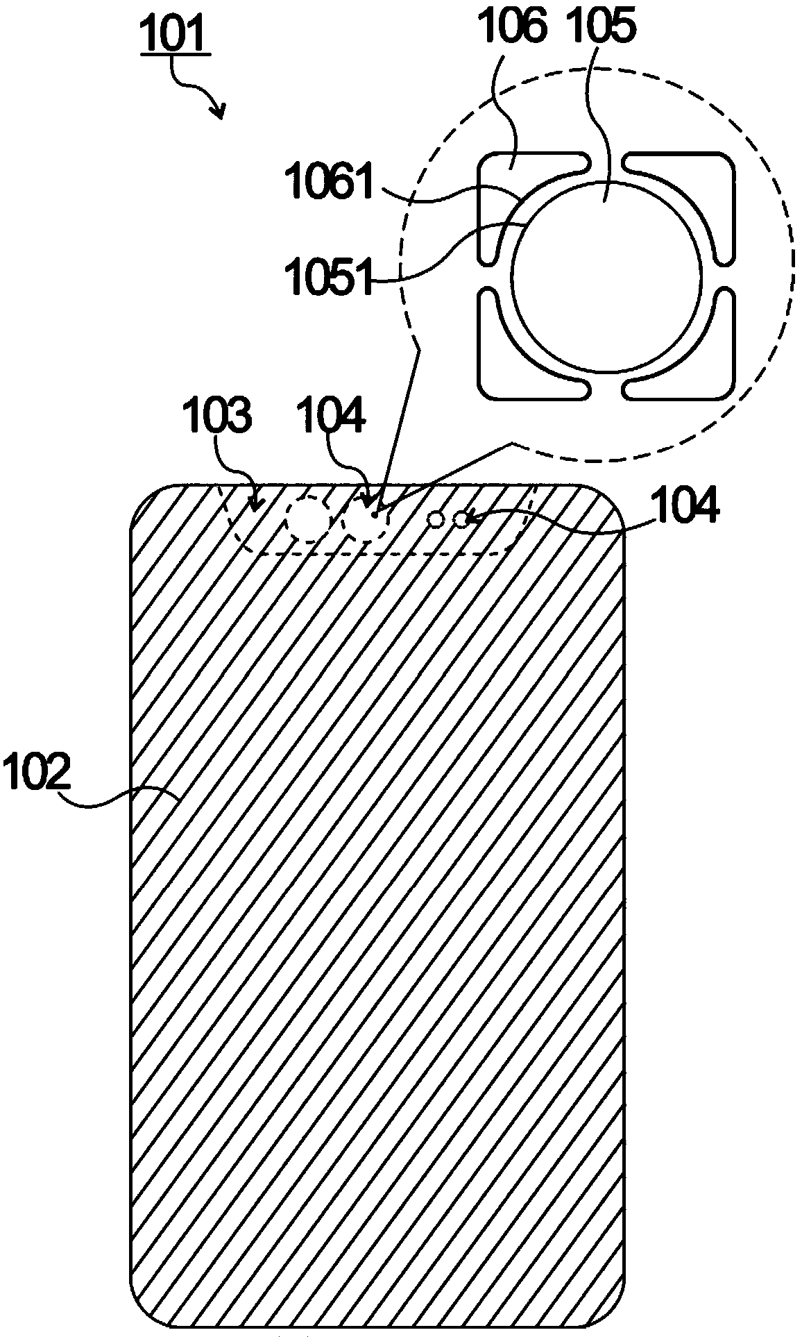
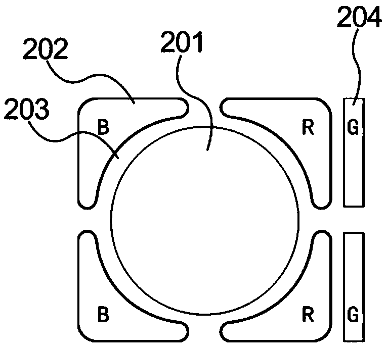
[0036] Such as Figure 2a As shown, the sensing area of ​​the OLED display panel is provided with a light-transmitting area 201, and a special-shaped sub-pixel 202 is arranged around the light-transmitting area 201, and a side of the special-shaped sub-pixel 202 facing the light-transmitting area 201 is provided with Depression 203 .

[0037] The outline of the light transmission area 201 is a circle formed by a closed arc, and the special-shaped sub-pixels 202 are symmetrically distributed around the light transmission area 201, and the shape of the special-shaped sub-pixels 202 is approximately a right triangle, The hypotenuse of the right triangle is an inner arc to form the concave portion 203 , and the hypotenuse is disposed toward the light-transmitting region 201 .

[0038] The two mutually perpendicular diameters of the light-transmitting region 201 include four diameter endpoints, and a position corresponding to each of the diameter endpoints is provided with a speci...

Embodiment 2

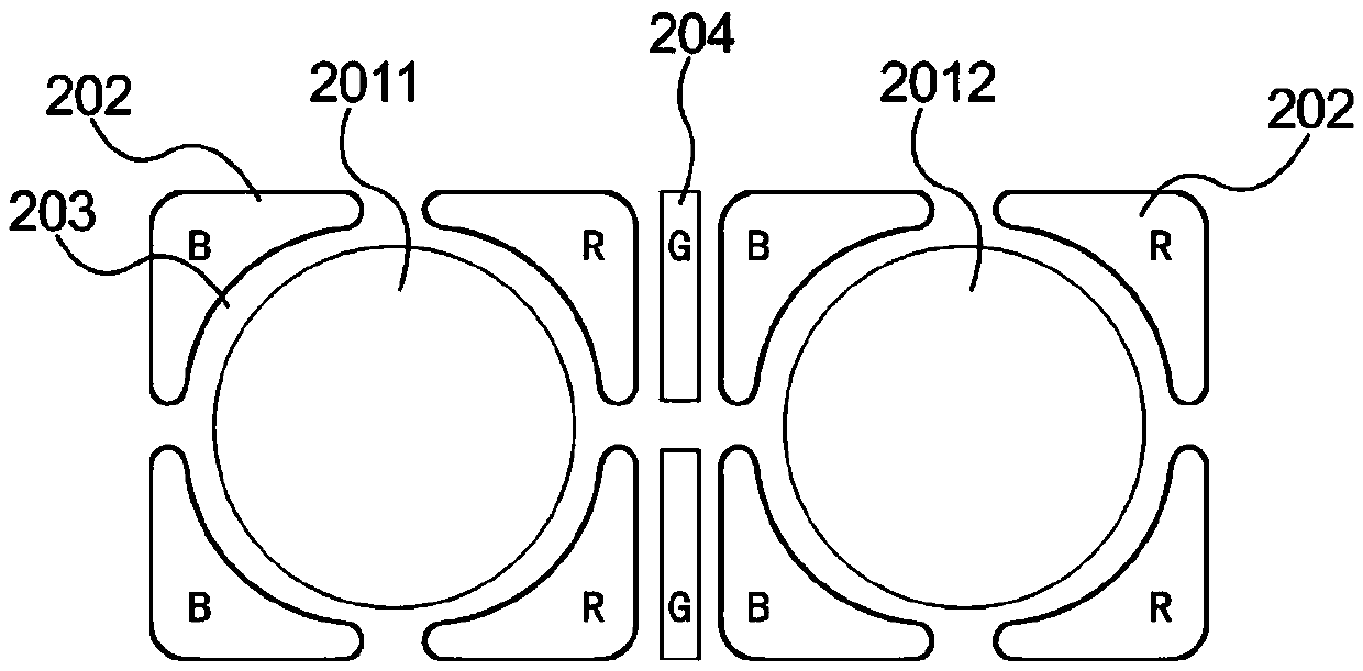
[0059] like image 3 As shown, the sensing area of ​​the OLED display panel is provided with a conventional sub-pixel 303, a light-transmitting area 301, and a special-shaped sub-pixel 306 located at the edge of the light-transmitting area 301, and the light-transmitting area 301 is surrounded by special-shaped sub-pixels 302 , a concave portion is disposed on at least one side of the shaped sub-pixel 302 facing the light-transmitting region 301 .

[0060] The outline of the light-transmitting region 301 is a circle formed by a closed arc, the irregular-shaped sub-pixels 302 are symmetrically distributed around the light-transmitting region 301 , and the two mutually perpendicular diameters of the light-transmitting region 301 Including four diameter endpoints, each of the corresponding positions of the diameter endpoints is provided with two of the special-shaped sub-pixels 302, and the arc length of the concave part of each of the special-shaped sub-pixels 302 is approximate...


PUM


Abstract

The invention provides an OLED display panel, which is characterized in that at least one light transmitting area for placing a photosensitive unit of a photosensitive element is formed in a display area, and special-shaped sub-pixels are arranged at the edge of the light transmitting area; wherein each special-shaped sub-pixel comprises at least one concave part, wherein the concave part is located on the side, facing the light-transmitting area, of the special-shaped sub-pixel, and the edge of the concave part corresponds to the edge of the light-transmitting area. Compared with the prior art, the OLED display panel provided by the invention has the advantages that the display pixels are expanded into the induction area, and the pixel shape of the edge of the light transmission area is optimized, so that the display area of the display panel is increased, and the image quality of the display panel is improved; the technical scheme solves the problems that according to an OLED displaypanel in the prior art, a large number of display pixels need to be sacrificed when an induction area is arranged, so that the display area of the display panel is reduced, and the display image quality of a screen is reduced.

Description

technical field [0001] The present invention relates to the field of display technology, in particular to an OLED display panel and a display device with the OLED display panel. Background technique [0002] Organic light-emitting diode (Organic Light-Emitting Diode, referred to as: OLED) display is gradually becoming the mainstream of the display industry due to its advantages such as wide viewing angle, high color gamut, and low power consumption. industry development goals. [0003] Nowadays, full-screen mobile phones have become the mainstream of the market. While increasing the screen ratio, the space of the sensing area is also squeezed. In order to optimize the setting space of the sensing area, the sensing device of the sensing area is usually set under the display panel. A notch matching the sensing area is provided on the surface of the display panel for setting the sensor device. The sensing area is provided with a plurality of permeable holes for exposing the ph...

Claims


Application Information

Patent Timeline
Patent Type & Authority Applications(China)
IPC IPC(8): H01L27/32
CPCG09F9/335H10K59/352H10K59/353H10K59/121
Inventor 周阳赵勇金武谦
Owner WUHAN CHINA STAR OPTOELECTRONICS SEMICON DISPLAY TECH CO LTD
Why Eureka
Try Eureka