Array substrate, display device and preparation method of array substrate

A technology for array substrates and display devices, which is applied in the direction of instruments, semiconductor devices, electrical components, etc., and can solve the problems that the display area cannot be fully utilized, the process is difficult, and the upper frame area of ​​​​the display panel is occupied.

Active Publication Date: 2018-09-18
KUNSHAN GO VISIONOX OPTO ELECTRONICS CO LTD
View PDF5 Cites 15 Cited by
  • Summary
  • Abstract
  • Description
  • Claims
  • Application Information

AI Technical Summary

Problems solved by technology

[0003] However, because the grooved area has a variety of cuts of different shapes, and when making the grooved area, it is necessary to cut each layer of substrate and film layer of the display panel, the process is very difficult; in addition, the g

Method used


Image

  • Array substrate, display device and preparation method of array substrate
  • Array substrate, display device and preparation method of array substrate
  • Array substrate, display device and preparation method of array substrate

Examples


Embodiment Construction

[0030] In order to make the above objects, features and advantages of the present invention more comprehensible, specific implementations of the present invention will be described in detail below in conjunction with the accompanying drawings. In the following description, numerous specific details are set forth in order to provide a thorough understanding of the present invention. However, the present invention can be implemented in many other ways different from those described here, and those skilled in the art can make similar improvements without departing from the connotation of the present invention, so the present invention is not limited by the specific embodiments disclosed below.

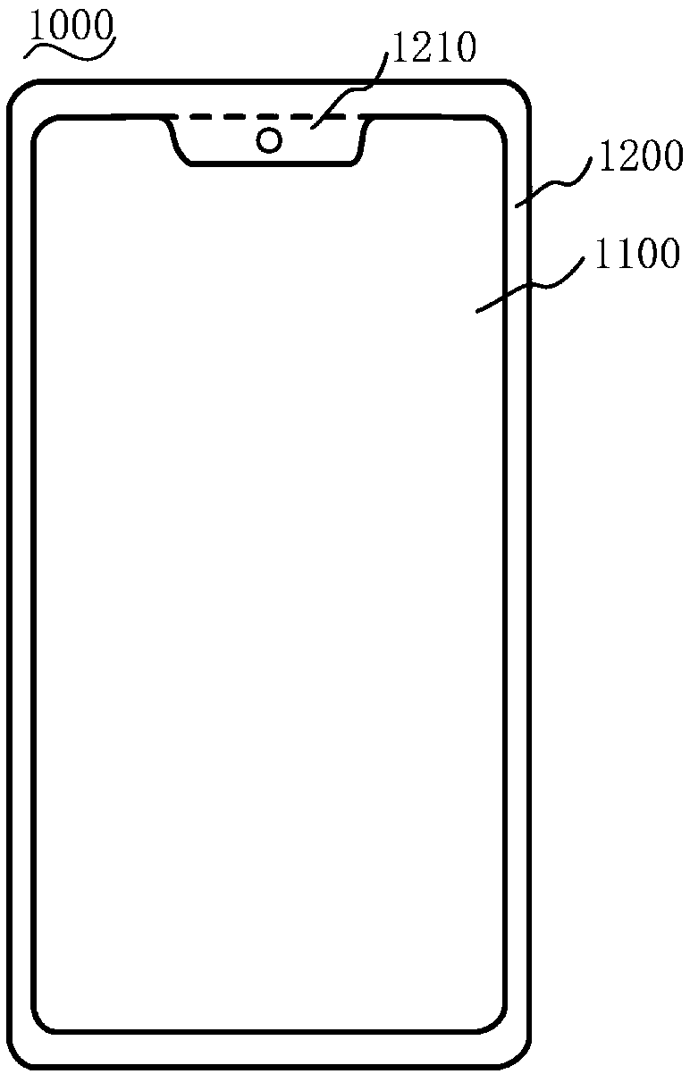
[0031] Please refer to figure 1 , which shows a schematic structural view of an embodiment of an array substrate according to the present application.

[0032] Such as figure 1 As shown, the array substrate 1000 includes a base substrate on which a display area 1100 and a non-display ar...


PUM


Abstract

The invention relates to an array substrate and a display device. The array substrate comprises a substrate base plate. A display region and a non-display region are arranged on the substrate base plate. The display region is sued for displaying. The non-display region comprises a groove region. The light transmittance of the groove region is larger than that of the display region. The display device comprises the array substrate. According to the invention, by setting the groove region on the substrate base plate, the making difficulty level of the groove region is reduced; and in addition, the groove region comprises the substrate base plate and is high in light transmittance, so circuits, components or signal lines can be placed in the groove space, frame area of the display region is reduced and display region of the display device is increased. The invention also relates to the method for preparing the array substrate.

Description

technical field [0001] The present invention relates to the field of display technology, in particular to an array substrate, a display device and a method for preparing the array substrate. Background technique [0002] With the continuous update and iteration of display device products, large-screen display devices are increasingly favored by users, and the external structure and internal structure of the display panel are constantly updated. Nowadays, one of the more popular methods is to make a slotted area on the top of the rectangular display panel where components such as the front camera can be placed, and make the display area in other areas except the slotted area, so as to increase The area of ​​the display area brings a stronger visual impact to the user. [0003] However, because the grooved area has a variety of cuts of different shapes, and when the grooved area is made, it is necessary to cut each layer of substrate and film layer of the display panel, the p...

Claims


Application Information

Patent Timeline
IPC IPC(8): H01L27/12G02F1/1333
CPCG02F1/1333H01L27/12H01L27/1214H01L27/1259
Inventor 周志伟黄秀颀胡思明宋艳芹李威龙韩珍珍
Owner KUNSHAN GO VISIONOX OPTO ELECTRONICS CO LTD
Why Eureka
Try Eureka