Array substrate and display panel

An array substrate and display direction technology, which is applied to static indicators, identification devices, instruments, etc., can solve the problems that camera equipment cannot accurately capture the relative positional relationship of two sets of alignment marks, and the longitudinal distance is large

Active Publication Date: 2020-08-21
WUHAN TIANMA MICRO ELECTRONICS CO LTD
View PDF19 Cites 11 Cited by
  • Summary
  • Abstract
  • Description
  • Claims
  • Application Information

AI Technical Summary

Problems solved by technology

[0005] In order to solve the above technical problems, the present application provides an array substrate and a display panel to solve the problem that the imaging equipment cannot accurately capture the relative position of the two sets of alignment marks due to the excessive longitudinal distance between the two sets of alignment marks after bending. The question of location

Method used


Image

  • Array substrate and display panel
  • Array substrate and display panel
  • Array substrate and display panel

Examples


Embodiment Construction

[0032] The following will clearly and completely describe the technical solutions in the embodiments of the application with reference to the drawings in the embodiments of the application. Apparently, the described embodiments are only some of the embodiments of the application, not all of them. Based on the embodiments in this application, all other embodiments obtained by persons of ordinary skill in the art without making creative efforts belong to the scope of protection of this application.

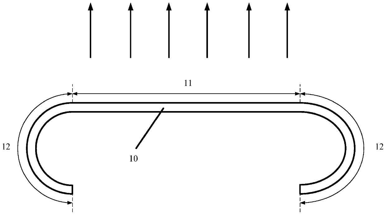
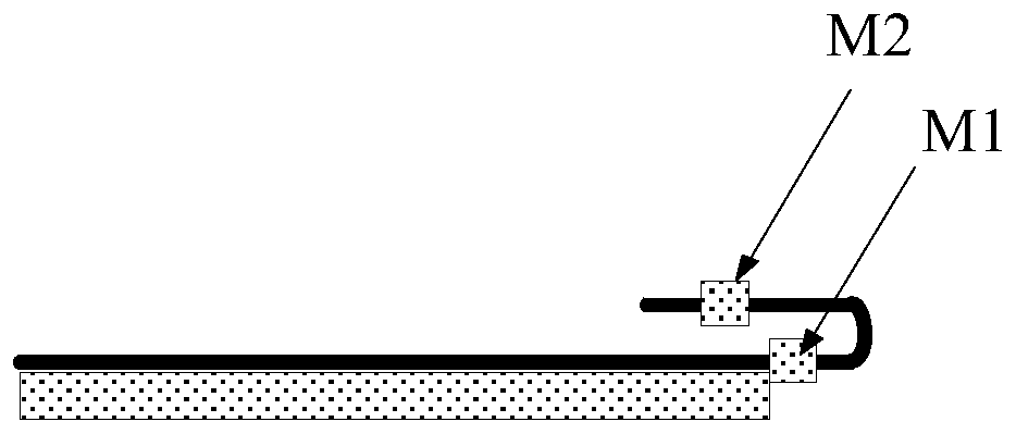
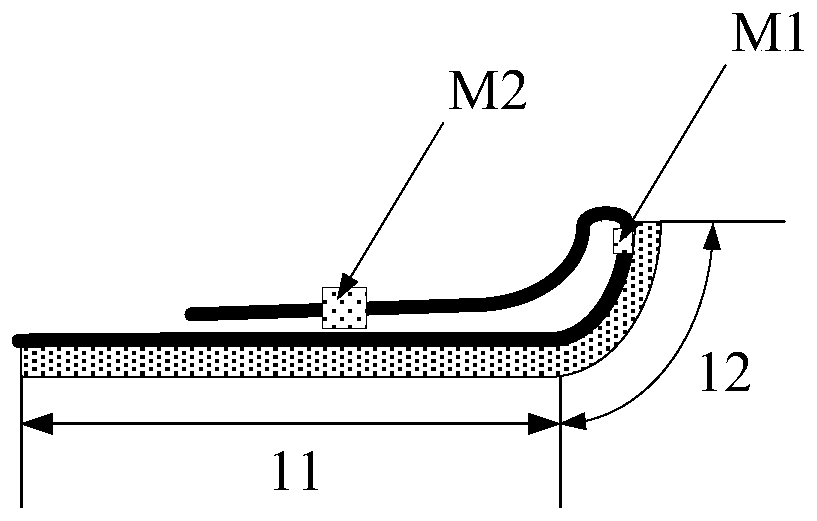
[0033] The embodiment of the present application provides an array substrate, refer to Figure 4 with Figure 5 , Figure 4 is a schematic plan view of the structure of the array substrate, Figure 5 It is a schematic cross-sectional structure diagram of the array substrate, and the array substrate includes:

[0034] The substrate 100, the substrate 100 includes a plane area 120 and a step area 110, the step area 110 includes a bending area 111 and a binding area 112, the bending...


PUM


Abstract

The invention discloses an array substrate and a display panel. A base of the array substrate comprises a plane area and a step area; the step area comprises a bending area and a binding area; a firstalignment mark and a second alignment mark are arranged on the surface of the substrate. The second alignment mark is arranged in the binding area. The first alignment mark is arranged in the plane area. The first alignment mark and any structural layer in the pixel structure are arranged on the same layer or the first alignment mark is located between the pixel structure and the substrate, so that the problem that the first alignment mark must be arranged in the bending area due to the absence of the arrangement position of the first alignment mark when all or most areas of the plane area are used for arranging the pixel structure is solved; thus, the problem that after the bending area is bent towards the side away from the display direction, the longitudinal distance between the firstalignment mark arranged in the bending area and the second alignment mark arranged in the step area is too large, and consequently a camera device cannot accurately grab the relative position relationbetween the first alignment mark and the second alignment mark is solved.

Description

technical field [0001] The present application relates to the field of display technology, and more specifically, to an array substrate and a display panel. Background technique [0002] With the continuous development of display technologies, the screen-to-body ratio of display devices continues to increase, and is constantly developing towards a true full screen. [0003] The emergence of flexible substrates provides a new solution for further increasing the screen-to-body ratio of display devices. Refer to figure 1 , figure 1 It is a schematic cross-sectional structure diagram of a flexible substrate 10 of a display device. In the display device, the flexible substrate 10 includes a planar region 11 and a step region 12 adjacent to the planar region 11. An array arrangement is arranged in the planar region 11. display pixels, the step area 12 is used to bind the chip or to set the wiring. After the chip or the wiring is set in the step area 12 of the flexible substrate ...

Claims


Application Information

Patent Timeline
Patent Type & Authority Applications(China)
IPC IPC(8): G09F9/30G09F9/33G09G3/32G09G3/3208H01L27/32
CPCG09F9/33G09G3/32G09G3/3208G09F9/301H10K59/88
Inventor 费日锂周瑞渊夏志强
Owner WUHAN TIANMA MICRO ELECTRONICS CO LTD
Why Eureka
Try Eureka