Check patentability & draft patents in minutes with Patsnap Eureka AI!

Memory control device

A control device and memory technology, which is applied in the field of circuit and PCB design, can solve the problems of long signal traces, difficult PCB wiring, adverse effects on signal integrity, etc., and achieves the effect of solving excessively long forks

Pending Publication Date: 2020-08-28
本征信息技术(苏州)有限公司
View PDF0 Cites 0 Cited by
  • Summary
  • Abstract
  • Description
  • Claims
  • Application Information

AI Technical Summary

Problems solved by technology

The cross-connection of a large number of signal lines and the increase in the number of through holes will cause certain difficulties in PCB routing, resulting in an increase in the number of layers, thickness and manufacturing cost of the PCB
Usually this also results in longer trace stubs on the front and back sides
For high-speed buses such as NAND Flash NVDDR3-1200 or SDRAM DDR4-3200, this will adversely affect signal integrity
Moreover, usually the signal trace lengths of the memory on the front and back sides of the PCB will also have a large difference, which is also unfavorable to the bus timing.

Method used


Image

  • Memory control device
  • Memory control device
  • Memory control device

Examples


Embodiment Construction

[0021] The principles and embodiments of the present invention will be described below in conjunction with the accompanying drawings. The specific examples are only used to explain the present invention, not to limit the scope of the present invention.

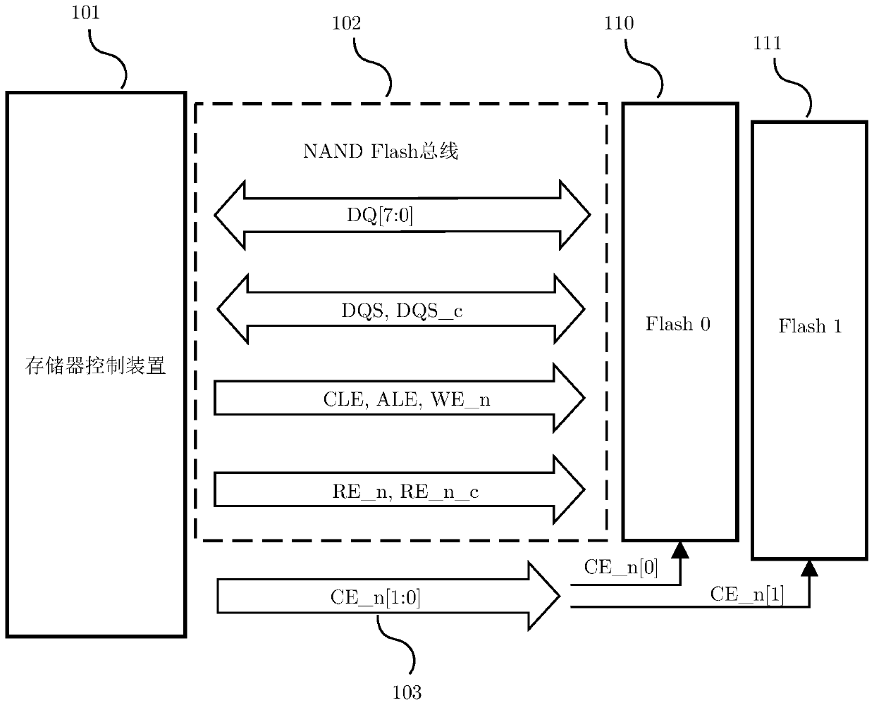
[0022] According to an embodiment of the present invention, image 3 It is a circuit block diagram of a memory control device. The memory control device 301 is connected to the memory 302 and the host 303 . The memory control device 301 receives commands from the host 303 , controls the memory 302 to perform operations such as read / write access, and returns command execution results to the host 303 .

[0023] The memory control device 301 includes:

[0024] one or more memory control logic 310;

[0025] one or more internal memory access buses 311;

[0026] one or more bus mirroring modules 320;

[0027] one or more bus configuration modules 312; and

[0028] One or more input / output modules 330 .

[0029] Wherein, the...


PUM


Abstract

A memory control apparatus includes one or more memory control logics, one or more memory buses, one or more bus mirroring modules, and one or more bus configuration modules. And the bus mirror imagemodule can change the bus signal connection relationship according to the bus configuration signal and the bus chip selection signal. Therefore, different signals, corresponding to different chip selection signals and having the same or similar pin positions, of the memories on the front and back surfaces of the PCB (printed circuit board) can share the same PCB wire. This helps to simplify the design of the PCB of the storage device and improve signal integrity and bus timing (timing).

Description

technical field [0001] The invention relates to the field of circuit and PCB design, in particular to a memory control device. Background technique [0002] In storage devices based on memory chips such as NAND Flash (flash memory), DRAM, PCM, RRAM, etc., usually a bus in the memory control device can be connected to multiple memory chips, and through chip select signals (such as CE_n or CS) signals to Select to access one of the memory chips. [0003] figure 1 It is a connection schematic diagram of a NAND Flash bus. A memory control device 101 is connected to two pieces of NAND Flash through a NAND Flash bus 102 . The bus signals include: data signal (DQ[7:0]), strobe signal (DQS, DQS_c), control signals such as CLE, ALE, WE_n, RE_n and RE_n_c, and chip select signal 103 . The two NAND Flashes are strobed through chip select signals CE_n[0] and CE_n[1] respectively. When CE_n[0] is low level and CE_n[1] is high level, NAND Flash 0110 is selected; when CE_n[0] is high ...

Claims


Application Information

Patent Timeline
Patent Type & Authority Applications(China)
IPC IPC(8): G11C5/06
CPCG11C5/063
Inventor 陈惕生
Owner 本征信息技术(苏州)有限公司
Features
  • R&D
  • Intellectual Property
  • Life Sciences
  • Materials
  • Tech Scout
  • Unparalleled Data Quality
  • Higher Quality Content
  • 60% Fewer Hallucinations
Learn More