

Deep silicon cavity etching method of micro-system module
A microsystem and deep etching technology, applied in the direction of microstructure technology, microstructure devices, manufacturing microstructure devices, etc., can solve the problems of different cavities, difficulty in adjusting the optimal etching passivation ratio, and increased production costs, and achieve Low cost, the effect of solving the problem of large cavity etching
- Summary
- Abstract
- Description
- Claims
- Application Information
AI Technical Summary
Problems solved by technology
Method used
Image

Examples
Embodiment 1
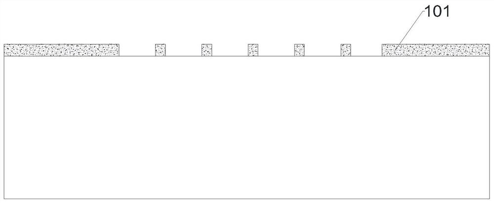
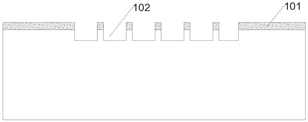
[0046] like Figure 1 to Figure 9 As shown, a method for etching a deep silicon cavity of a microsystem module specifically includes the following steps:
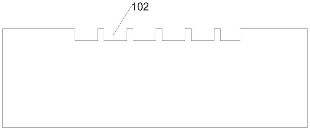
[0047] 101) Preliminary etching step: coating a photoresist 101 on the upper surface of the wafer, the thickness of the photoresist 101 ranging from 8 microns to 15 microns. Distribute and form at least two or more preliminary cavities on the photoresist 101 through exposure and development technology, the opening size of the preliminary cavities is between 20 microns and 50 microns, and the etching depth is increased, and the etching depth is 20 microns to 80 microns After the etching is completed, the photoresist 101 is removed to form a corresponding small cavity 102 . The photoresist 101 here can be a positive resist or a negative resist, and the coating of the photoresist 101 can be a dry film pasted on the wafer or a liquid photoresist 101 spin-coated on the wafer. Etching can be wet etching or dry etching.
[0048...
Embodiment 2
[0053] Such as Figure 8 to Figure 16 As shown, a method for etching a deep silicon cavity of a microsystem module specifically includes the following steps:
[0054] 101) Preliminary etching step: deposit a layer of hard mask layer 105 with a thickness ranging from 2 to 10 microns on the upper surface of the wafer, form a preliminary large cavity 104 on the hard mask layer 105 by exposure and development technology, and The etching depth is increased to form a corresponding large cavity 107 .
[0055] The hard mask layer 105 here can adopt various suitable deposition methods such as chemical vapor deposition, physical vapor deposition, and evaporation. The thickness of the deposited hard mask layer 105 can be adjusted arbitrarily to meet good performance requirements. The hard mask layer 105 can be made of various materials with hard mask properties such as silicon dioxide and silicon nitride. The pattern etched out of the hard mask layer 105 can be etched by dry etching o...
Embodiment 3
[0061] Such as Figure 8 , Figure 9 , Figure 17 to Figure 20 As shown, a deep silicon cavity etching method for a microsystem module, the specific test process is as follows:
[0062] 101) Preliminary etching step: coating photoresist 101 on the upper surface of the wafer, the coating thickness ranges from 8 microns to 15 microns, and distributes at least two or more preliminary cavities on the photoresist 101 through exposure and development technology, And the etching depth is increased to form a small cavity 102, and the depth of the small cavity 102 is between 8 microns and 15 microns. The gluing method can be spin coating method or dry film pasting method; the width of the small cavity 102 and the side wall thickness of the small cavity 102 can be adjusted arbitrarily to meet good performance requirements.
[0063] 102) Preliminary shaping step: further increase the etching depth on the processed wafer in step 101), remove the photoresist 101 after the etching is com...
PUM
| Property | Measurement | Unit |
|---|---|---|
| thickness | aaaaa | aaaaa |
| thickness | aaaaa | aaaaa |
| size | aaaaa | aaaaa |
Abstract
Description
Claims
Application Information