A through-hole structure and manufacturing method thereof

A conductive structure and blind hole technology, which is applied in semiconductor/solid-state device manufacturing, semiconductor/solid-state device components, semiconductor devices, etc., can solve problems such as difficult process implementation

Active Publication Date: 2015-10-14
NAT CENT FOR ADVANCED PACKAGING CO LTD
View PDF3 Cites 0 Cited by
  • Summary
  • Abstract
  • Description
  • Claims
  • Application Information

AI Technical Summary

Problems solved by technology

However, due to the limitations of the process, some process steps can only complete the processing of TSVs with an aspect ratio less than 10:1, such as CVD insulating layer, PVD seed layer and electroplating filling, etc.
If you make a TSV structure with an aspect ratio greater than 10:1, it is currently difficult to achieve in terms of technology

Method used


Image

  • A through-hole structure and manufacturing method thereof
  • A through-hole structure and manufacturing method thereof
  • A through-hole structure and manufacturing method thereof

Examples


Embodiment Construction

[0032] Embodiments of the present invention are described in detail below.

[0033] Examples of the described embodiments are shown in the drawings, wherein like or similar reference numerals designate like or similar elements or elements having the same or similar functions throughout. The embodiments described below by referring to the figures are exemplary only for explaining the present invention and should not be construed as limiting the present invention. To simplify the disclosure of the present invention, components and arrangements of specific examples are described below. Of course, they are only examples and are not intended to limit the invention.

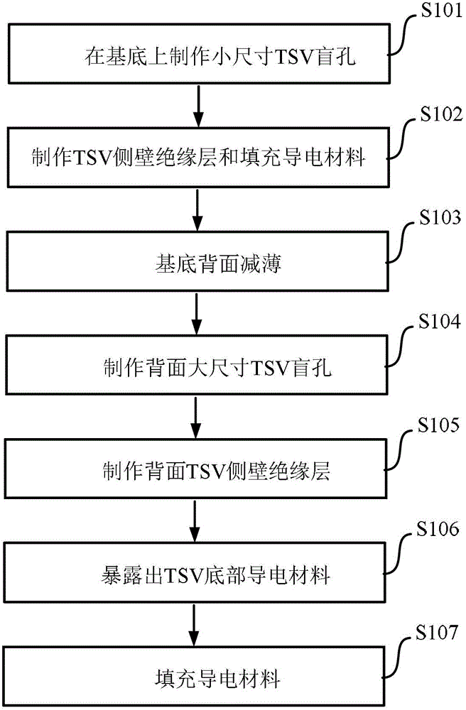
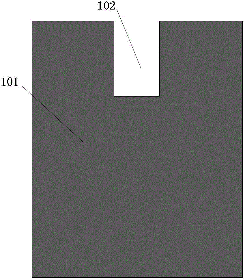
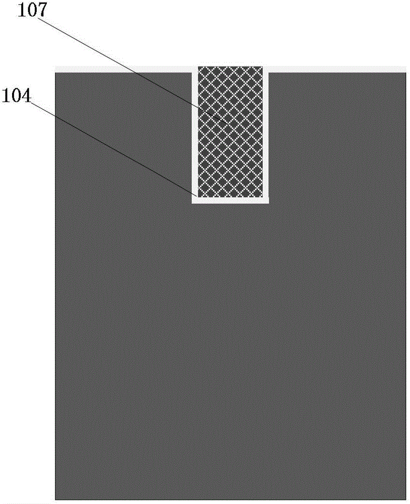
[0034] According to one aspect of the present invention, a method for fabricating a TSV with a high aspect ratio or an ultra-high aspect ratio is provided. Below, will combine Figure 2 to Figure 7 A method for forming the structure is specifically described through an embodiment of the present invention. like fig...


PUM


Abstract

The invention relates to a manufacturing method of a TSV (through silicon via) used in an interposer adapter plate in 2.5 D or 3D packaging. The method is characterized in that a TSV structure is formed by double-sided etching and double-sided filling. The method disclosed by the invention can be used for forming the TSV structure with a high depth-width ratio or ultrahigh depth-width ratio. A variety of limitations of the TSV structure with the high depth-width ratio or ultrahigh depth-width ratio in the aspects of a formation process, equipment, finished product rate and reliability can be further solved. Correspondingly, the invention further provides a TSV structure.

Description

technical field [0001] The invention relates to microelectronic packaging technology and 3D IC technology, in particular to a method for manufacturing a TSV structure used in interposer adapter board technology. technical background [0002] 3D-TSV integration technology is one of the core technologies of microelectronics. 3D-TSV interconnection provides a method beyond "Moore". It is currently the most advanced and complex packaging technology; it can obtain better electrical performance, low power consumption, noise, smaller package size, low cost, and versatility. 3D-TSV technology will be widely used in the field of microelectronics, especially consumer electronics such as smartphones, including high-end products such as smartphones, Internet of Things devices, sensors, memories, solar cells, LEDs, and power devices. [0003] At present, among many new 3D packaging technologies that have emerged, TSV technology is a key technology for multi-chip stacked integration and ...

Claims


Application Information

Patent Timeline
Patent Type & Authority Patents(China)
IPC IPC(8): H01L23/48H01L21/768
Inventor 曹立强戴风伟
Owner NAT CENT FOR ADVANCED PACKAGING CO LTD
Why Eureka
Try Eureka