Contact hole etching method, integrate circuit (IC) manufacturing method and IC

A contact hole etching and integrated circuit technology, which is applied in the direction of circuit, semiconductor/solid-state device manufacturing, electrical components, etc., can solve the problems of semiconductor device leakage, insufficient etching, contact hole connection, etc.

Active Publication Date: 2014-06-11
SHANGHAI HUALI MICROELECTRONICS CORP
View PDF4 Cites 0 Cited by
  • Summary
  • Abstract
  • Description
  • Claims
  • Application Information

AI Technical Summary

Problems solved by technology

On the one hand, if the amount of overetching is too small during etching, it may cause insufficient etching in the overlapped area, which may cause contact hole connection problems
On the other hand, if the amount of overetching is too much, it may cause the problem of leakage of semiconductor devices in the single-layer contact hole etch stop layer (also used as a stress layer)

Method used


Image

  • Contact hole etching method, integrate circuit (IC) manufacturing method and IC
  • Contact hole etching method, integrate circuit (IC) manufacturing method and IC
  • Contact hole etching method, integrate circuit (IC) manufacturing method and IC

Examples


Embodiment Construction

[0023] In order to make the content of the present invention clearer and easier to understand, the content of the present invention will be described in detail below in conjunction with specific embodiments and accompanying drawings.

[0024] The following will refer to Figure 1 to Figure 5 A contact hole etching method according to an embodiment of the present invention will be described. As shown in the figure, the contact hole etching method according to the embodiment of the present invention includes the following steps:

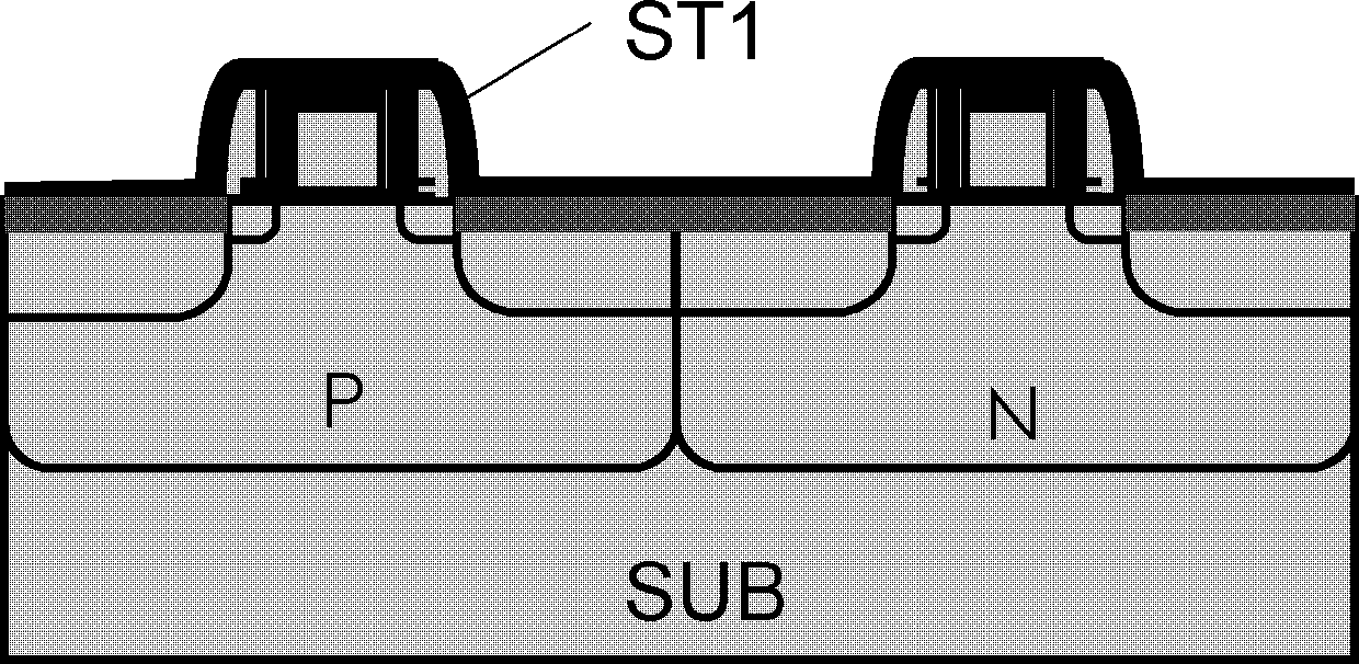
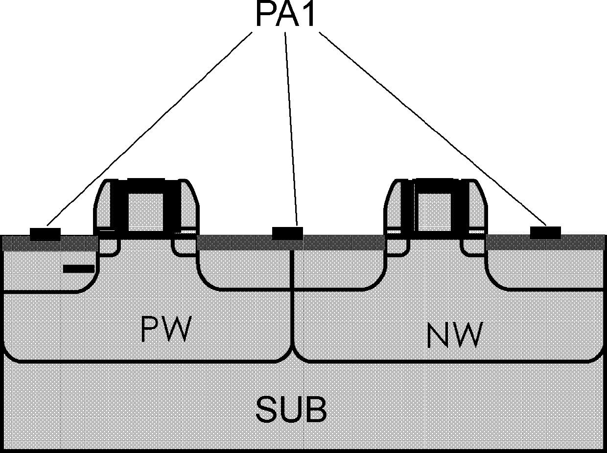
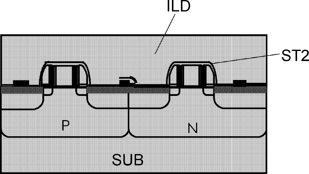
[0025] The first contact hole etch stop layer forming step is used to form the first contact hole etch stop layer ST1. figure 1 A schematic diagram schematically shows a step of forming a first contact hole etching barrier layer in a contact hole etching method according to an embodiment of the present invention. Such as figure 1 As shown, a P well PW and an N well NW are arranged on the semiconductor substrate SUB; specifically, the P well PW is us...


PUM


Abstract

The invention provides a contact hole etching method, an integrate circuit (IC) manufacturing method and an IC. The contact hole etching method comprises the following steps: a first contact hole etching barrier layer formation step: forming a first contact hole etching barrier layer; an etching step of the first contact hole etching barrier layer: using a first mask to etch the first contact hole etching barrier layer so as to keep the first contact hole etching barrier layer on a position where the contact hole is about to be formed; a second contact hole etching barrier layer formation step: forming the second contact hole etching barrier layer after the etching step of the first contact hole etching barrier layer; an internal layer dielectric layer formation step: forming an internal layer dielectric layer on the second contact hole etching barrier layer; a contact hole etching step: using a second mask to etch the internal layer dielectric layer so as to form the contact hole; a contact hole filling step: using a conductive material to fill in the contact hole which is etched through the contact hole etching step.

Description

technical field [0001] The invention relates to the field of integrated circuit manufacturing, in particular to a contact hole etching method, an integrated circuit manufacturing method using the contact hole etching method, and an integrated circuit manufactured by the integrated circuit manufacturing method. Background technique [0002] For the manufacture of integrated circuits (IC, integrate circuit), semiconductor devices (active devices and / or passive devices) are generally manufactured in wafers (also called wafers), and then metal The wiring layer is wired to connect semiconductor devices to form integrated circuits or modules with certain functions. [0003] In order to form an integrated circuit or chip, contact holes are required to realize the electrical connection between the semiconductor device and the metal layer. The contact holes are generally formed by etching. [0004] In the contact hole etching method in the prior art, the hole etch stop layer and th...

Claims


Application Information

Patent Timeline
Patent Type & Authority Patents(China)
IPC IPC(8): H01L21/768H01L21/311
Inventor 石磊
Owner SHANGHAI HUALI MICROELECTRONICS CORP
Why Eureka
Try Eureka