Display panel, manufacturing method thereof, and display device

A technology for display panels and substrates, applied in semiconductor devices, electrical components, circuits, etc., can solve the problems of the lifespan of the quantum dot color conversion layer and the effect of color conversion efficiency, and achieve the effect of improving reliability, quality and quality.

Active Publication Date: 2021-12-07
BOE TECH GRP CO LTD
View PDF5 Cites 0 Cited by
  • Summary
  • Abstract
  • Description
  • Claims
  • Application Information

AI Technical Summary

Problems solved by technology

[0004] The present invention aims at the current problem that the high temperature of Micro LEDs affects the lifespan and color conversion efficiency of the quantum dot color conversion layer, and provides a display panel and its preparation method and display device

Method used


Image

  • Display panel, manufacturing method thereof, and display device
  • Display panel, manufacturing method thereof, and display device

Examples


Embodiment Construction

[0034] In order to enable those skilled in the art to better understand the technical solution of the present invention, a display panel, a manufacturing method thereof, and a display device of the present invention will be further described in detail below in conjunction with the accompanying drawings and specific embodiments.

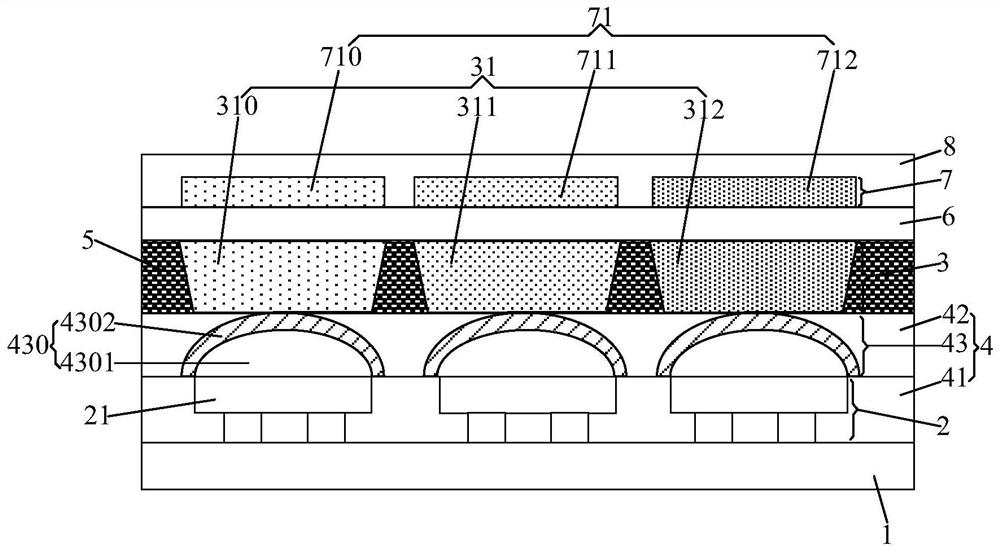
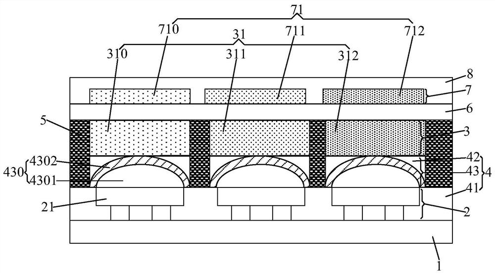
[0035] In a current public technology, the quantum dot color conversion layer is directly coated on the cover plate by adopting a “pair box” structure, the quantum dot color conversion layer is arranged in an array, and the quantum dot color conversion layer and the quantum dot color conversion layer are arranged in an array. Each MicroLED sub-pixel corresponds to one-to-one, and the cover plate is covered on the substrate where the MicroLED sub-pixel is located to form a closed structure. The box-shaped closed structure is airtight, and the actual working temperature of Micro LED is 80-120°C. High temperature has a great influence on the lifespan and ...


PUM

PropertyMeasurementUnit
thermal conductivityaaaaaaaaaa

Abstract

The invention provides a display panel, a preparation method thereof, and a display device. The display panel includes a substrate, a light-emitting unit array and a quantum dot color film array arranged on the substrate, the quantum dot color film array is located on the light-emitting side of the light-emitting unit array, and the quantum dot color film and the light-emitting unit array The light-emitting units correspond one-to-one; a blocking structure is also included, and the blocking structure is arranged between the light-emitting unit array and the quantum dot color film array to prevent the heat emitted by the light-emitting unit from being conducted to the quantum dot color film. The display panel can improve or avoid the working temperature of the light-emitting unit having a greater impact on the lifespan and color conversion efficiency of the quantum dot color film by setting a blocking structure, thereby improving or avoiding the overall reliability of the quantum dot color film caused by the heat dissipation of the light-emitting unit Performance (such as lifespan and color conversion efficiency) is reduced, and the quality of the display panel is improved.

Description

technical field [0001] The invention belongs to the field of display technology, and in particular relates to a display panel, a preparation method thereof, and a display device. Background technique [0002] MicroLEDs are achieved by employing an array of LEDs, where each pixel is much smaller than conventional LEDs. Its applications include smartwatch / smartphone displays, tablets, laptops, monitors, TVs, and NEDs (Near Eye Displays) such as AR / VR (Augmented Reality / Virtual Reality). However, Micro LED is limited by the complexity of the process and the problem of transfer yield, and the overall production cost is high. [0003] At present, through the integration of single blue MicroLED and quantum dot (QD) color conversion layer, the purpose of simplifying the process route, improving yield and reducing production cost is achieved. However, for the current Micro LED display products, the working temperature of Micro LED is 80-120°C. High temperature has a great impact o...

Claims


Application Information

Patent Timeline
Patent Type & Authority Patents(China)
IPC IPC(8): H01L33/48H01L33/50H01L33/58H01L33/64H01L27/15
CPCH01L33/48H01L33/507H01L33/58H01L33/64H01L27/156H01L25/0753H01L25/167H01L33/644H01L2933/0075H01L2933/0041H01L2933/0058H01L27/1248H01L33/56H01L33/641H01L2933/005
Inventor 田禹靳倩孙倩黄维
Owner BOE TECH GRP CO LTD
Why Eureka
Try Eureka