
Manufacturing method of PCB

A production method and prepreg technology, which is applied in multilayer circuit manufacturing, printed circuit manufacturing, electrical components, etc., can solve the problems of complex manufacturing process, uneven groove bottom, and low depth control accuracy, and achieve simple manufacturing process and accurate depth Controllable, smooth effect

Inactive Publication Date: 2020-09-25
DONGGUAN SHENGYI ELECTRONICS
View PDF5 Cites 1 Cited by
  • Summary
  • Abstract
  • Description
  • Claims
  • Application Information

AI Technical Summary

Problems solved by technology

[0004] The purpose of the present invention is to provide a PCB manufacturing method to simultaneously overcome the defects of uneven groove bottom, low depth control precision and complex manufacturing process existing in the existing groove manufacturing process

Method used


Image

  • Manufacturing method of PCB
  • Manufacturing method of PCB
  • Manufacturing method of PCB

Examples


Embodiment 1

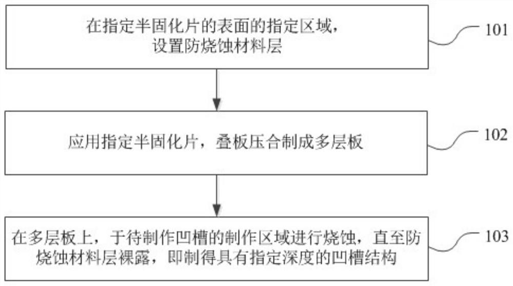
[0040] see figure 1 and figure 2 , the manufacturing method of the PCB that the embodiment of the present invention provides, comprises steps:

[0041] Step 101, setting an anti-ablation material layer 2 on a designated area on the surface of the designated prepreg 1 .

[0042] Wherein, the designated prepreg 1 refers to the prepreg located at the bottom of the groove of the PCB to be made. The specified area refers to the projection area of ​​the groove to be made on the surface of the specified semi-solid sheet. According to the preset manufacturing requirements, the groove to be made has a specified depth; at the same time, the shape and size of the cross section of the groove to be made are not specifically limited.

[0043] The anti-ablation material layer 2 is made of materials that cannot or are difficult to be ablated by laser. Specifically, a material with ablation energy greater than that required by the prepreg can be selected, and it is soluble and can pass thr...

Embodiment 2

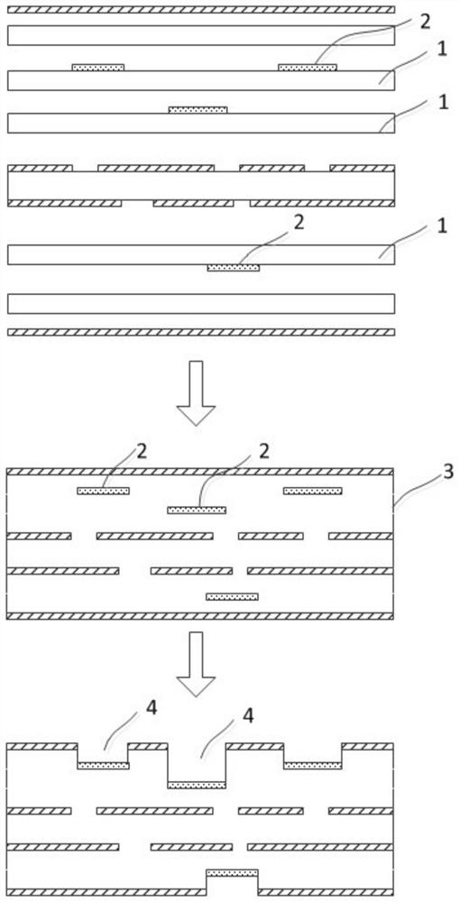
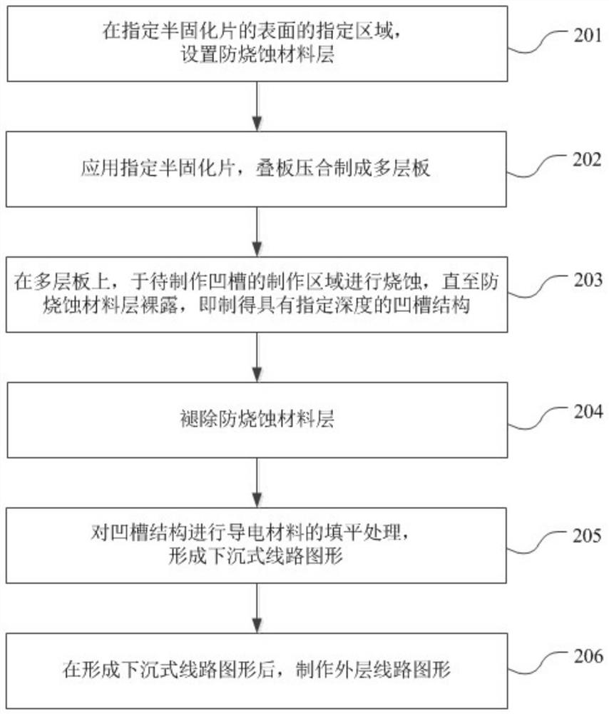
[0053] see image 3 and Figure 4 , the embodiment of the present invention provides another PCB manufacturing method, including steps:

[0054] Step 201, setting an anti-ablation material layer 2 on a designated area on the surface of the designated prepreg 1 .

[0055] In this embodiment, the anti-ablation material layer 2 is specifically an ink layer, which is coated on the surface of the specified prepreg 1 with a certain thickness.

[0056] Step 202 , apply the specified prepreg 1 , and press the laminated boards to form a multi-layer board 3 .

[0057] Step 203 , on the multi-layer board 3 , perform ablation in the region where the groove is to be made until the anti-ablation material layer 2 is exposed, that is, a groove structure 4 with a specified depth is made.

[0058] Step 204 , removing the anti-ablation material layer 2 .

[0059] Since the anti-ablation material layer 2 of this embodiment is ink, it can be removed by developing and etching with liquid medicine...


PUM


Abstract

The invention relates to the technical field of PCBs, and discloses a manufacturing method of a PCB. The method comprises the following steps that: anti-ablation material layers are arranged in specified areas on the surfaces of specified prepregs, the specified prepregs are prepregs located at the groove bottom of a groove to be manufactured, and the specified areas are the projection areas of the grooves to be manufactured on the surface of the specified prepregs, wherein the groove to be manufactured has a specified depth; the specified prepregs are laminated and pressed into a multilayer board; and on the multilayer board, the manufacturing area of the groove to be manufactured is ablated until the anti-ablation material layers are exposed, so that a groove structure with the specifieddepth can be obtained. According to the embodiment of the invention, the prepregs at the bottom of the groove to be manufactured are pretreated before lamination and pressing; in the laser ablation process, the anti-ablation material layers 2 achieve a good ablation blocking function due to the fact that the anti-ablation material layers 2 cannot be ablated or is difficult to ablate, so that thedepth of the groove structure formed after ablation is accurate and controllable, the flatness of the groove bottom is ensured, and the manufacturing process is simple.

Description

technical field [0001] The present invention relates to the technical field of PCB (Printed Circuit Board, printed circuit board), in particular to a method for manufacturing a PCB. Background technique [0002] PCB is one of the important electronic components in the electronics industry. It is not only the carrier of electronic components, but also the provider of electrical interconnection between electronic components. Nowadays, PCB has developed from the initial single-layer board to double-sided board and multi-layer board, among which multi-layer board is widely used because of its high assembly density, small size, high signal transmission speed, and easy wiring. [0003] At present, the manufacturing process of grooves on multilayer boards usually has the following types: direct laser ablation, controlled depth milling, and embedding gaskets. However, there are various defects in these methods, for example: the bottom of the groove made by direct laser ablation is ...

Claims


Application Information

Patent Timeline
IPC IPC(8): H05K3/00H05K3/46H05K3/18
CPCH05K3/0026H05K3/18H05K3/4644
Inventor 林宇超刘梦茹王洪府纪成光陈正清
Owner DONGGUAN SHENGYI ELECTRONICS
Learn More