Display panel and display device

A display panel and display surface technology, which is applied in the direction of instruments, acquisition/organization of fingerprints/palmprints, optical components, etc., can solve the problems of low transmittance, low brightness, and difficulty in satisfying optical fingerprint recognition, etc.

Active Publication Date: 2020-10-09
WUHAN CHINA STAR OPTOELECTRONICS TECH CO LTD
7 Cites 7 Cited by

AI-Extracted Technical Summary

Problems solved by technology

[0003] For Organic Light-Emitting Diode (OLED), due to its self-luminous characteristics and high transmittance of the light-emitting layer, it meets the conditions of fingerprint recognition and is easy to realize fingerprint recognition under the screen, but for Liquid Crystal Display (Liquid Crystal Display) , LCD), because it requires ...

Method used

[0035] Wherein, the display surface 101a is used for displaying a picture, and the non-display surface 101b is the side opposite to the display surface 101a, and is not used for displaying a picture. The fingerprint identification area 101c refers to the area where fingerprint information is collected during fingerprint identification, and the non-fingerprint identification area 101d refers to the area of ​​the display screen 101 outside the fingerprint identification area 101c, where the screen can still be displayed during fingerprint identification. For example, as shown in FIG. 1 , the fingerprint identification area 101c is a circular area in the display screen 101 , and the area of ​​the display screen 101 other than the circle is a non-fingerprint identification area. In FIG. 1 , the non-fingerprint identification area 101d is set around the fingerprint identification area 101c as an example, which is not intended to limit the positional relationship and shape of the fingerprint identification area 101c and the non-fingerprint identification area 101d in this application. Wherein, the first backlight module 102 is set corresponding to the non-fingerprint identification area 101d, and the second backlight module 103 is set corresponding to the fingerprint identification area 101c. Specifically, in the setting method shown in FIG. 1 , the position and shape of the first backlight module 102 are completely consistent with the non-fingerprint identification area 101d. The position of the second backlight module 103 is consistent with the fingerprint identification area 101c, but the shape of the second backlight module 103 may not be completely consistent with the fingerprint identification area 101c, for example, the second backlight module 103 may partially exceed the fingerprint identification area 101c, to The seamless connection between the second backlight module 103 and the first backlight module 102 is realized to obtain a better full-screen display image. The fingerprint sensor 104 is disposed in the fingerprint identification area 101c or completely corresponding to the fingerprint identification area 101c, so as to improve the efficiency of fingerprint identification.
[0039] Please refer to FIG. 2. FIG. 2 is a first cross-sectional schematic view of the display panel 10 provided by the embodiment of the present application. Wherein, the first backlight module 102 is arranged on the non-display surface 101b, and the second backlight module 103 is arranged on the side of the first backlight module 102 away from the non-display surface 101b. Setting the first backlight module 102 at a position close to the display screen 101 reduces the loss of the backlight of the first backlight module 102 during the transmission process, improves the utilization rate of light, and enables the display screen 101 to obtain better display effects .
[0040] Please refer to FIG. 3. FIG. 3 is a second cross-sectional schematic diagram of the display panel 10 provided by the embodiment of the present application. The second backlight module 102 is disposed on the non-display surface 101b, and the first backlight module 102 is disposed on a side of the second backlight module 103 away from the non-display surface 101b. Setting the second backlight module 102 close to the display screen 101 can enable the fingerprint sensor 104 to better identify fingerprint signals and obtain more accurate identification results.
[0041] Wherein, since the firs...

Abstract

The embodiment of the invention provides a display panel. The display panel comprises a display screen, a first backlight module, a second backlight module and a fingerprint sensor. The second backlight module has a fingerprint identification mode and a display mode, in the fingerprint identification mode, light penetrates through the second backlight module to reach the fingerprint sensor to perform fingerprint identification, and in the display mode, the second backlight module and the first backlight module provide uniform backlight for the display screen. By arranging the second backlightmodule, the display panel can achieve the function of being compatible with under-screen fingerprint recognition and display.

Application Domain

Substation equipmentPrint image acquisition +2

Technology Topic

Computer hardwareFinger print +2

Image

  • Display panel and display device
  • Display panel and display device
  • Display panel and display device

Examples

  • Experimental program(1)

Example Embodiment

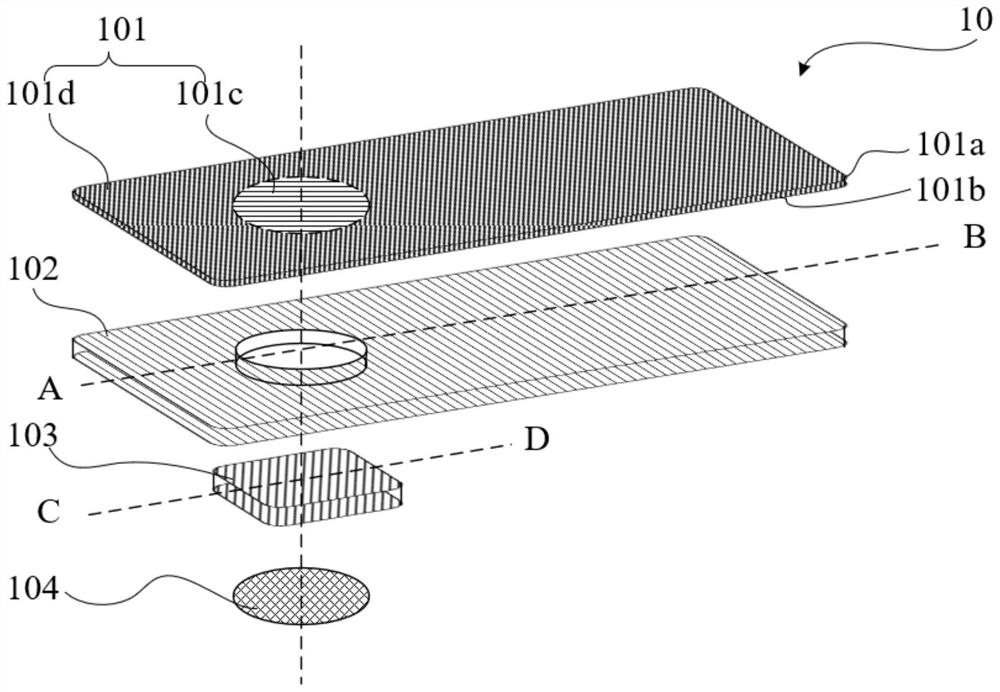
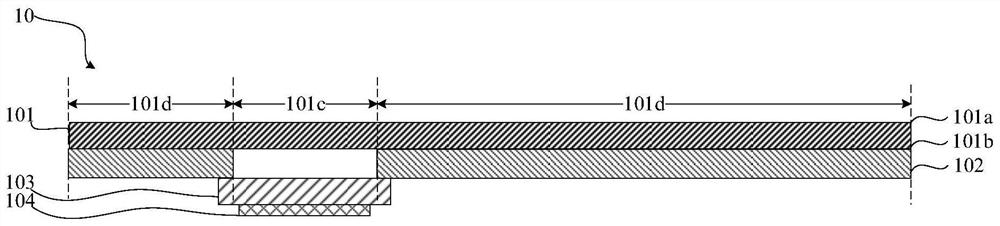
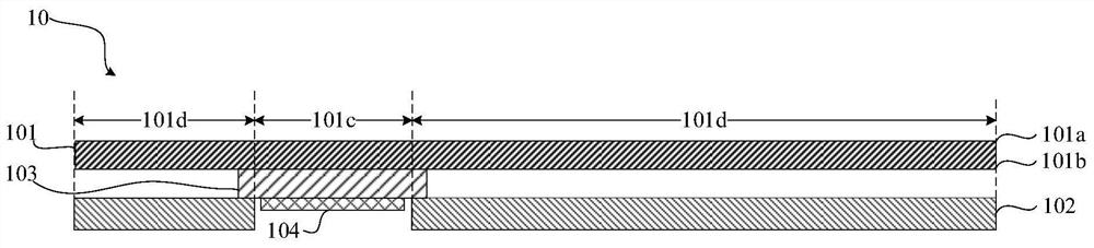
[0031] The technical solutions in the embodiments of the present application will be clearly and completely described below in conjunction with the drawings in the embodiments of the present application. Obviously, the described embodiments are only a part of the embodiments of the present application, rather than all the embodiments. Based on the embodiments in this application, all other embodiments obtained by those skilled in the art without creative work are within the protection scope of this application.
[0032] It should be noted that in the description of this application, it should be understood that the terms "upper", "lower", "front", "rear", "left", "right", "inner", "outer", etc. The indicated orientation or positional relationship is based on the orientation or positional relationship shown in the drawings, which is only for the convenience of describing the application and simplifying the description, and does not indicate or imply that the pointed device or element must have a specific orientation or a specific orientation. The structure and operation cannot therefore be understood as a limitation of this application.
[0033] The embodiments of the present application provide a display panel, a display panel manufacturing method, and a display device. The display panel will be described in detail below.
[0034] See figure 1 , figure 1 It is a schematic diagram of the structure of the display panel 10 provided by an embodiment of the present application. The display panel 10 includes a display screen 101, a first backlight module 102, a second backlight module 103, and a fingerprint sensor 104. The display screen 101 has a display surface 101a and a non-display surface 101b, and also has a fingerprint recognition area 101c and a fingerprint recognition area The non-fingerprint recognition area 101d other than 101c. The first backlight module 102 is disposed on the non-display surface 101b, and the first backlight module 102 is disposed corresponding to the non-fingerprint recognition area 101d. The second backlight module 103 and the first backlight module 102 are arranged on the same side of the display screen 101 and connected to the first backlight module 102, and the second backlight module 103 is arranged corresponding to the fingerprint recognition area 101c. The fingerprint sensor 104 is arranged on the side of the second backlight module 103 away from the display screen 101.
[0035] Among them, the display surface 101a is used for displaying a screen, and the non-display surface 101b is a surface opposite to the display surface 101a and is not used for displaying a screen. The fingerprint recognition area 101c refers to the area where fingerprint information is collected during fingerprint recognition, and the non-fingerprint recognition area 101d refers to the area outside the fingerprint recognition area 101c in the display screen 101, and the screen can still be displayed during fingerprint recognition. For example, such as figure 1 As shown, the fingerprint identification area 101c is a circular area in the display screen 101, and the area of ​​the display screen 101 other than the circle is a non-fingerprint identification area. figure 1 Taking the non-fingerprint recognition area 101d around the fingerprint recognition area 101c as an example, it does not limit the positional relationship and shape of the fingerprint recognition area 101c and the non-fingerprint recognition area 101d in this application. Among them, the first backlight module 102 is provided corresponding to the non-fingerprint recognition area 101d, and the second backlight module 103 is provided corresponding to the fingerprint recognition area 101c. Specifically, in figure 1 In the setting method shown, the position and shape of the first backlight module 102 are completely consistent with the non-fingerprint recognition area 101d. The position of the second backlight module 103 is consistent with the fingerprint recognition area 101c, but the shape of the second backlight module 103 may not be completely consistent with the fingerprint recognition area 101c. For example, the second backlight module 103 may partially extend beyond the fingerprint recognition area 101c to The seamless connection between the second backlight module 103 and the first backlight module 102 is realized, and a better full-screen display image is obtained. The fingerprint sensor 104 is arranged in the fingerprint identification area 101c or is arranged at a position completely corresponding to the fingerprint identification area 101c, so as to improve the efficiency of fingerprint identification.
[0036] Among them, the second backlight module 103 has a fingerprint recognition mode and a display mode. In the fingerprint recognition mode, light passes through the second backlight module 103 to the fingerprint sensor 104 and performs fingerprint recognition. In the display mode, the second backlight module 103 and the first backlight module 102 provide uniform backlight to the display screen 101.
[0037] Specifically, in the fingerprint recognition mode, the second backlight module 103 is in a non-transparent state, and the backlight provided by the second backlight module 103 is totally reflected in the second backlight module 103. Therefore, the light reflected by the finger during fingerprint recognition can pass through the second backlight module 103 to reach the fingerprint sensor 104 to realize fingerprint recognition. In the display mode, the second backlight module 103 is in a transparent state, and the backlight provided by the second backlight module 103 is uniformly scattered in the second optical module 103 like the first backlight module 102, so the second backlight module 103 can provide uniform backlight to the display screen 101 together with the first backlight module 102 to realize a full-screen display.
[0038] The display panel 10 provided by the embodiment of the present application is provided with a second backlight module 103 having a fingerprint recognition mode and a display mode in the fingerprint recognition area 101d, and the second backlight module 103 can allow light to pass through and reach the fingerprint in the fingerprint recognition mode. The sensor 104 performs fingerprint recognition. In the display mode, the second backlight module 103 and the first backlight module 102 provide uniform backlight to the display screen 101 to achieve full-screen display. Therefore, the display panel 10 provided by the embodiment of the present application can be compatible with under-screen fingerprint recognition and display functions.
[0039] See figure 2 , figure 2 It is a schematic diagram of the first cross-sectional structure of the display panel 10 provided by an embodiment of the present application. The first backlight module 102 is arranged on the non-display surface 101b, and the second backlight module 103 is arranged on the side of the first backlight module 102 away from the non-display surface 101b. Arranging the first backlight module 102 at a position close to the display screen 101 reduces the loss of the backlight of the first backlight module 102 during the propagation process, improves the light utilization rate, and enables the display screen 101 to obtain better display effects .
[0040] See image 3 , image 3 It is a schematic diagram of the second cross-sectional structure of the display panel 10 provided by an embodiment of the present application. The second backlight module 102 is arranged on the non-display surface 101b, and the first backlight module 102 is arranged on the side of the second backlight module 103 away from the non-display surface 101b. Arranging the second backlight module 102 close to the display screen 101 can enable the fingerprint sensor 104 to better recognize fingerprint signals and obtain more accurate recognition results.
[0041] Wherein, since the first backlight module 102 is arranged on the side of the fingerprint sensor 104 away from the display screen 101, the first backlight module 102 can also be arranged in a whole-surface structure (not shown in the drawings), which does not affect fingerprint recognition. It can also provide backlight in the non-fingerprint recognition area 101d. Deploying the first backlight module 102 as a whole-surface structure can reduce manufacturing steps, reduce manufacturing difficulty, save production costs, and improve production efficiency.
[0042] See Figure 4 , Figure 4 It is a schematic diagram of the third cross-sectional structure of the display panel 10 provided by the embodiment of the present application. Wherein, the first backlight module 102 and the second backlight module 103 are arranged on the non-display surface 101b, and the first backlight module 102 and the second backlight module 103 are arranged on the same layer. Such a setting method can make the light obtained by the display screen 101 more uniform in the display mode, thereby achieving a better full-screen display effect. Moreover, the arrangement of the first backlight module 102 and the second backlight module 103 in the same layer can reduce the thickness of the display panel 10.
[0043] Wherein, when the fingerprint recognition area 101c is at one end or edge of the display screen 101 (not shown in the figure), the position of the second backlight module 103 corresponding to the fingerprint recognition area 101c can be set at one end of the first backlight module 102 , Thereby reducing the manufacturing process steps of the first backlight module 102. For example, the first backlight module 102 and the second backlight module 103 can be arranged on the same substrate, and the first backlight module 102 and the second backlight module 103 obtains an integrated structure through the entire surface manufacturing process, which simplifies the production process.
[0044] See Figure 5 , Figure 5 It is a schematic diagram of the second backlight module 103 along the CD cross-section structure provided by the embodiment of the present application. The second backlight module 103 includes an optical element 103a and a second light source 103b. The optical element 103a switches the fingerprint recognition mode and In the display mode, the second light source 103b is arranged on at least one side surface of the optical element 103a.
[0045] Wherein, the second light source 103b is any one of a light emitting diode, a mini light emitting diode, or a small cold cathode fluorescent lamp. Light-emitting diodes, mini light-emitting diodes or small cold-cathode fluorescent lamps constitute a point light source and a fire-ray light source. The second light source 103b may be a visible light source or a mixed light source of visible light and infrared light. The light-emitting diode or mini light-emitting diode has a long service life. Among them, the mini light-emitting diode occupies a small volume and can be arranged more on the side of the optical element 103a to make the light more uniform. The small cold cathode fluorescent lamp has high brightness, which can reduce the influence of the loss in light transmission on the final display effect.
[0046] Among them, the optical element 103a includes a first substrate 1031, a second substrate 1033, and an interlayer material 1032 disposed between the first substrate 1031 and the second substrate 1033. The interlayer material 1032 is capable of switching between transparent and transparent states under voltage control. Non-transparent materials.
[0047] Among them, the first substrate 1031 and the second substrate 1033 are rigid substrates or flexible substrates. The materials used for the first substrate 1031 and the second substrate 1033 are glass, polyethylene terephthalate (PET, Polyethylene terephthalate) or polyimide (PI, Polyimide). The materials of the first substrate 1031 and the second substrate 1033 and the materials used can be the same or different, and can be set according to the requirements of the display panel 10.
[0048] Among them, the interlayer material 1032 is a polymer dispersed liquid crystal (PDLC, Polymer Dispersed Liquid Crystal) or a polymer network liquid crystal (PNLC, Polymer Network Liquid Crystal). The above materials can realize the change of transparent state and non-transparent state under voltage control. After the second backlight module 103 is connected to the integrated circuit through a signal line or a flexible circuit board, the voltage is changed in the fingerprint recognition mode and the display mode to change the state of the interlayer material 1032, thereby achieving the compatibility of the fingerprint recognition and display functions under the screen.
[0049] Specifically, in the fingerprint recognition mode, the interlayer material 1032 is controlled by the voltage to transform into a non-transparent state, and the light from the second light source 103b is totally reflected in the optical element 103a. Therefore, the light reflected by the finger during fingerprint recognition can pass through the second backlight module 103 to reach the fingerprint sensor 104, and fingerprint recognition is realized. In the display mode, the interlayer material 1032 is controlled by voltage to transform into a transparent state, and the light from the second light source 103b is uniformly scattered in the optical element 103a, so the second backlight module 103 and the first backlight module 102 can share the display screen 101 provides uniform backlight to achieve full screen display.
[0050] The optical element 103a has a first display area 103c and a second display area 103d, and the second display area 103d is arranged around the first display area 103c. The second display area 103d with uniform scattering is arranged around the first display area 103c and connected to the first backlight module 102, so that the second backlight module 103 and the display screen of the first backlight module 102 can be seamlessly connected.
[0051] Specifically, see Image 6 , Image 6 It is a schematic diagram of the working principle of the fingerprint recognition mode provided by the embodiment of the present application. In fingerprint recognition mode, such as Image 6 As shown, the light from the second light source 103b is totally reflected in the first display area 103c, and the light from the second light source 103b is uniformly scattered in the second display area 103d. Since the backlight of the first display area 103c is totally reflected, during fingerprint recognition, the light reflected by the finger can pass through the first display area 103c to reach the fingerprint sensor 104 to realize fingerprint recognition.
[0052] Or, in the fingerprint recognition mode, control the second light source 103b to turn off, and ensure that the fingerprint recognition state time is very short, so that the human eye cannot recognize the turn off of the second light source 103b.
[0053] Specifically, see Figure 7 , Figure 7 It is a schematic diagram of the working principle of the display mode provided by the embodiment of the present application. In the display mode, light from the second light source 103d is uniformly scattered in the first display area 103c and the second display area 103d. It is used to provide uniform backlight to the display screen 101 for screen display.
[0054] The brightness of the second light source 103b in the fingerprint recognition mode is greater than the brightness of the second light source 103b in the display mode. In the fingerprint recognition mode, increasing the brightness of the second light source 103b can increase the light intensity sensed by the fingerprint sensor, thereby improving the performance and accuracy of fingerprint recognition.
[0055] See Figure 8 , Figure 8 It is a schematic diagram of the structure of the first backlight module 102 along the A-B section provided by the embodiment of the present application. The first backlight module 102 includes a prism sheet 1021, a diffusion sheet 1022, a light guide plate 1023, a reflection sheet 1024, and a first light source 1025. The prism sheet 1021, the diffusion sheet 1022, the light guide plate 1023, and the reflection sheet 1024 are along a direction away from the display screen 101 They are stacked in sequence, and the first light source 1025 is disposed on at least one side surface of the light guide plate 1023.
[0056] Among them, the prism sheet 1021 is used to improve the luminous efficiency of the entire backlight system. The diffusion sheet 1022 can be used to enhance the optical taste, and can also be used to improve the adsorption of the film and other parts of the display panel 10. The light guide plate 1023 is used to lead out the first light source 1025, where the first light source 1025 is any one of a light emitting diode, a mini light emitting diode, or a small cold cathode fluorescent lamp. The light guide plate 1023 converts the point light source of the light emitting diode or mini light emitting diode into a surface light source, and then provides a uniform backlight to the display screen 101. The reflective sheet 1024 is used to control the reflection and refraction of light, so that the light path can be controlled, and the brightness of the display panel 10 can be more uniform. The provision of the above film layers can enable the display panel 10 to achieve a better display effect with lower power consumption.
[0057] among them, Figure 8 The non-fingerprint recognition area 101d shown is arranged around the fingerprint recognition area 101c, so the first backlight module 102 digs a hole in the fingerprint recognition area 101c to vacate the fingerprint recognition area 101c. Specifically, the first backlight module 102 may be digged in the fingerprint recognition area 101c through a process such as photolithography or etching. In addition, to facilitate the manufacturing process, the first backlight module 102 can be fabricated in the non-fingerprint recognition area 101d, and the transparent substrate can be reserved in the fingerprint recognition area 101c. For example, a halftone mask process is used to provide the first backlight module in the non-fingerprint recognition area 101d. The backlight module 102, as long as it does not affect the passing of the fingerprint identification signal.
[0058] Wherein, in the display mode, the brightness of the first light source 1025 is the same as the brightness of the second light source 103b. In the display mode, in order to achieve a uniform display of the full screen, the brightness of the first light source 1025 and the brightness of the second light source 103b are adjusted to be consistent, which can achieve a better display effect.
[0059] The embodiment of the present application provides a display device 100, Picture 9 It is a schematic diagram of the structure of the display device 100 in an embodiment of the present application. The display device 100 includes the above-mentioned display panel 10 and the circuit structure 20, and the display device 100 may also include other devices. The circuit structure 20 and other devices and their assembly in the embodiments of the present application are related technologies well known to those skilled in the art, and will not be repeated here.
[0060] The display device 100 provided by the embodiment of the present application includes a display panel 10 and a circuit structure 20. The display panel 10 is provided with a first backlight module 102 and a second backlight module 103 in a fingerprint recognition area 101c and a non-fingerprint recognition area 101d, respectively. , Through the second backlight module 103 to perform different state adjustments in the fingerprint recognition mode and the display mode, the compatibility of the fingerprint recognition and display functions under the screen is realized.
[0061] The display panel and the display device provided by the embodiments of the present application are described in detail above. Specific examples are used in this article to illustrate the principles and implementations of the present application. The description of the above embodiments is only used to help understand the present application. At the same time, for those skilled in the art, according to the idea of ​​the application, there will be changes in the specific implementation and the scope of application. In summary, the content of this specification should not be construed as a limitation of the application.

PUM

no PUM

Description & Claims & Application Information

We can also present the details of the Description, Claims and Application information to help users get a comprehensive understanding of the technical details of the patent, such as background art, summary of invention, brief description of drawings, description of embodiments, and other original content. On the other hand, users can also determine the specific scope of protection of the technology through the list of claims; as well as understand the changes in the life cycle of the technology with the presentation of the patent timeline. Login to view more.
Why Eureka
Try Eureka