Transmitting terminal of high-definition digital image transmission system of traversing machine
A digital image and transmission system technology, applied in the field of traversing machines, can solve problems such as less information, inability to use traversing machines, and blurred images, and achieve the effects of avoiding image cross-linking, improving player controllability, and reducing weight
- Summary
- Abstract
- Description
- Claims
- Application Information
AI Technical Summary
Problems solved by technology
Method used
Image

Examples
Embodiment Construction
[0034] The following will clearly and completely describe the technical solutions in the embodiments of the present invention with reference to the accompanying drawings in the embodiments of the present invention. Obviously, the described embodiments are only some, not all, embodiments of the present invention. Based on the embodiments of the present invention, all other embodiments obtained by persons of ordinary skill in the art without making creative efforts belong to the protection scope of the present invention.
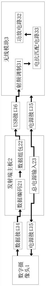
[0035] see figure 1, a transmitting end of a high-definition digital image transmission system of a traversing machine, comprising a digital camera 1, a transmitting end main board 2, a wireless module 3, a data interface 4, a power supply interface 5 and a USB interface 6, and the transmitting end main board 2 contains a data code 21, a data Group package 22 and total power input 23, wireless module 3 contains radio frequency modulation 31, reactance matching...
PUM
 Abstract
Description
Claims
Application Information
 - R&D
- Intellectual Property
- Life Sciences
- Materials
- Tech Scout
- Unparalleled Data Quality
- Higher Quality Content
- 60% Fewer Hallucinations
Browse by: Latest US Patents, China's latest patents, Technical Efficacy Thesaurus, Application Domain, Technology Topic, Popular Technical Reports.
© 2025 PatSnap. All rights reserved.Legal|Privacy policy|Modern Slavery Act Transparency Statement|Sitemap|About US| Contact US: help@patsnap.com