Method for debouncing an electrical input signal, and debouncing module
A technology of input signal and output signal, applied in the field of anti-jitter module, can solve problems such as long delay
- Summary
- Abstract
- Description
- Claims
- Application Information
AI Technical Summary
Problems solved by technology
Method used
Image

Examples
Embodiment Construction
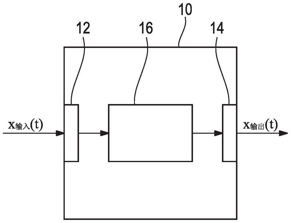
[0042] figure 1 Shown is a debouncing module 10 having a function for receiving an electrical input signal x 输入 (t) signal input terminal 12, for outputting electrical output signal x 输出 (t) the signal output terminal 14 and the signal processing unit 16 .
[0043] The signal processing unit 16 is arranged in such a manner as to be connected downstream of the signal input terminal 12 , and is signal-transmittingly connected to the signal input terminal 12 . Further, the signal processing unit 16 is arranged in such a manner as to be connected upstream of the signal output terminal 14 , and is connected to the signal output terminal 14 in a signal transmission manner.
[0044] In general, the signal processing unit 16 is designed to receive an electrical input signal x via a signal input 12 输入 , to process the input signal x 输入 and based on the input signal x 输入 generate the output signal x 输出 .
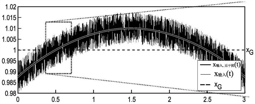
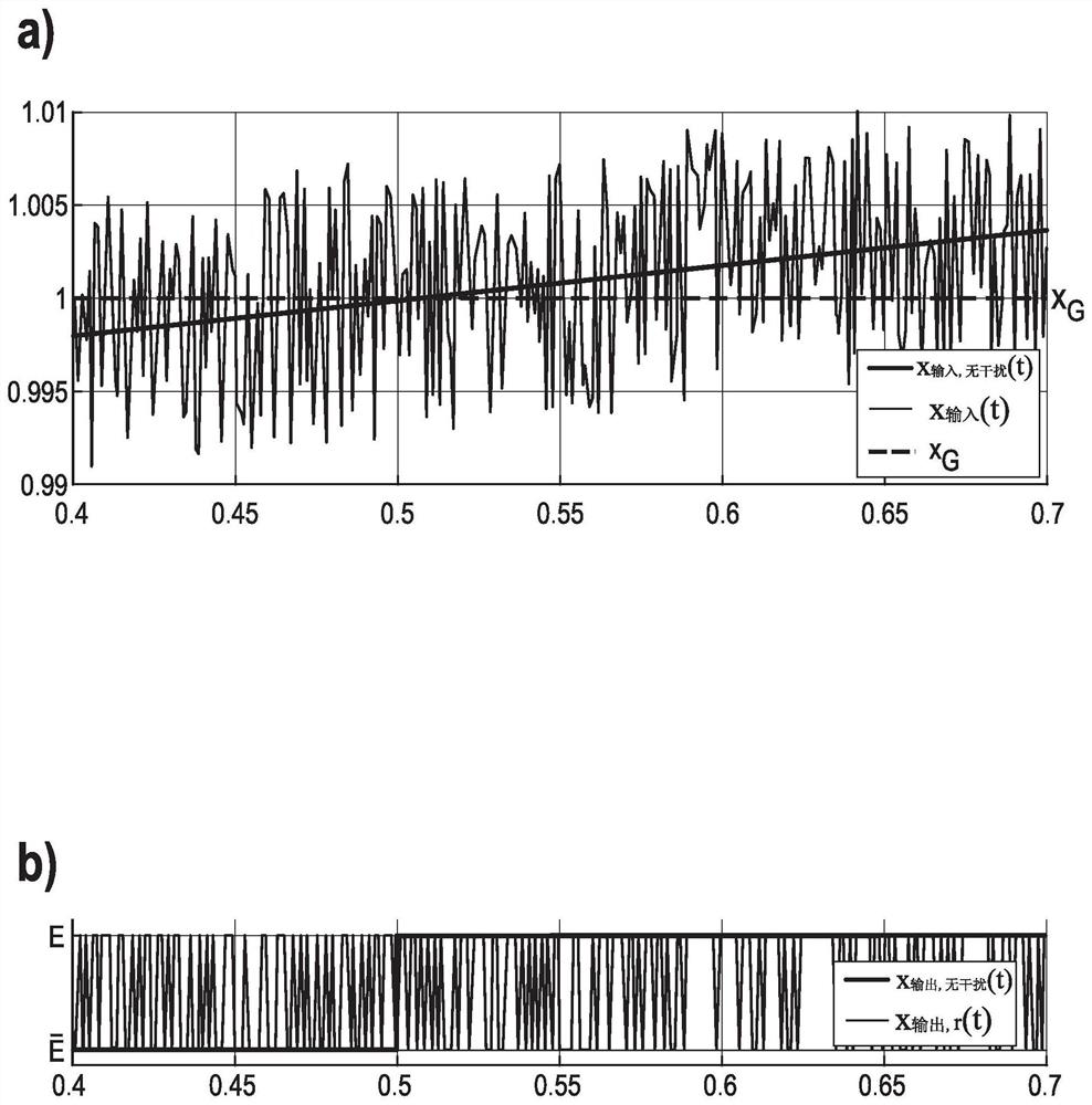
[0045] figure 2 The input signal x is shown plotted against time t 输入 E...
PUM
 Abstract
Description
Claims
Application Information