Data reading circuit and storage unit
A technology of data reading and reading unit, which is applied in the field of integrated circuits, can solve the problems of small data reading and reading margin, and achieve the effect of improving the reading margin
- Summary
- Abstract
- Description
- Claims
- Application Information
AI Technical Summary
Problems solved by technology
Method used
Image

Examples
Embodiment Construction
[0024] In the prior art, excessive current may rewrite the data stored in the MRAM, resulting in read disturbance (Read Disturb). Therefore, the requirement on the voltage bias of the bit line of the MRAM cell is relatively high, and when the read voltage of the bit line is small, the read current is also small, which will result in a large read error.
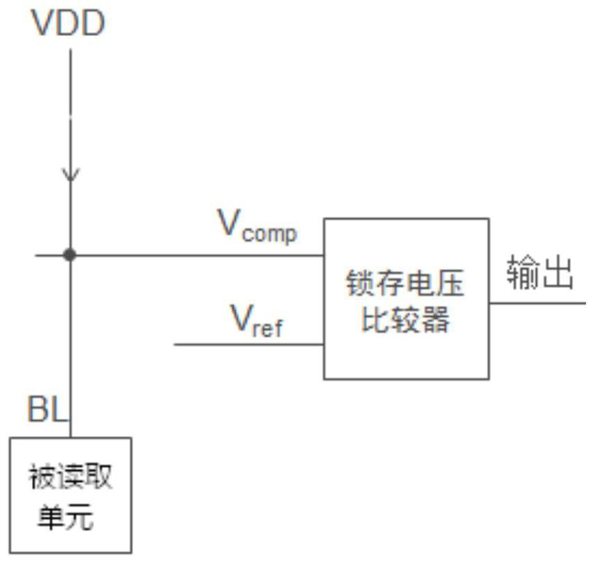
[0025] refer to figure 1 , a circuit structure diagram of an existing data reading circuit is given.
[0026] The existing data reading circuit includes a read unit and a latch voltage comparator. Depend on figure 1 It can be seen that the voltage comparison point V comp Connect directly to the bit line BL of the cell being read. at the voltage comparison point V comp with reference voltage V ref When the input latch voltage comparator is used for comparison, the bit line BL voltage is affected by the current of the cell being read (VDD is the power supply voltage), which in turn causes the voltage comparison point V co...
PUM
 Abstract
Description
Claims
Application Information
 - R&D
- Intellectual Property
- Life Sciences
- Materials
- Tech Scout
- Unparalleled Data Quality
- Higher Quality Content
- 60% Fewer Hallucinations
Browse by: Latest US Patents, China's latest patents, Technical Efficacy Thesaurus, Application Domain, Technology Topic, Popular Technical Reports.
© 2025 PatSnap. All rights reserved.Legal|Privacy policy|Modern Slavery Act Transparency Statement|Sitemap|About US| Contact US: help@patsnap.com