Semiconductor integrated circuit having connection down-lead for bit line interconnection

A technology for connecting wires and semiconductors, which is applied in the field of reliable reading data, and can solve problems such as yield decline, manufacturing cost increase, and read margin reduction

Inactive Publication Date: 2007-03-21
FUJITSU MICROELECTRONICS LTD
View PDF5 Cites 0 Cited by
  • Summary
  • Abstract
  • Description
  • Claims
  • Application Information

AI Technical Summary

Problems solved by technology

Therefore, the reduction in read margin results in a decrease in yield
In turn, lower yields lead to higher manufacturing costs

Method used


Image

  • Semiconductor integrated circuit having connection down-lead for bit line interconnection
  • Semiconductor integrated circuit having connection down-lead for bit line interconnection
  • Semiconductor integrated circuit having connection down-lead for bit line interconnection

Examples


Embodiment Construction

[0039] Specific embodiments of the present invention will be described below with reference to the accompanying drawings.

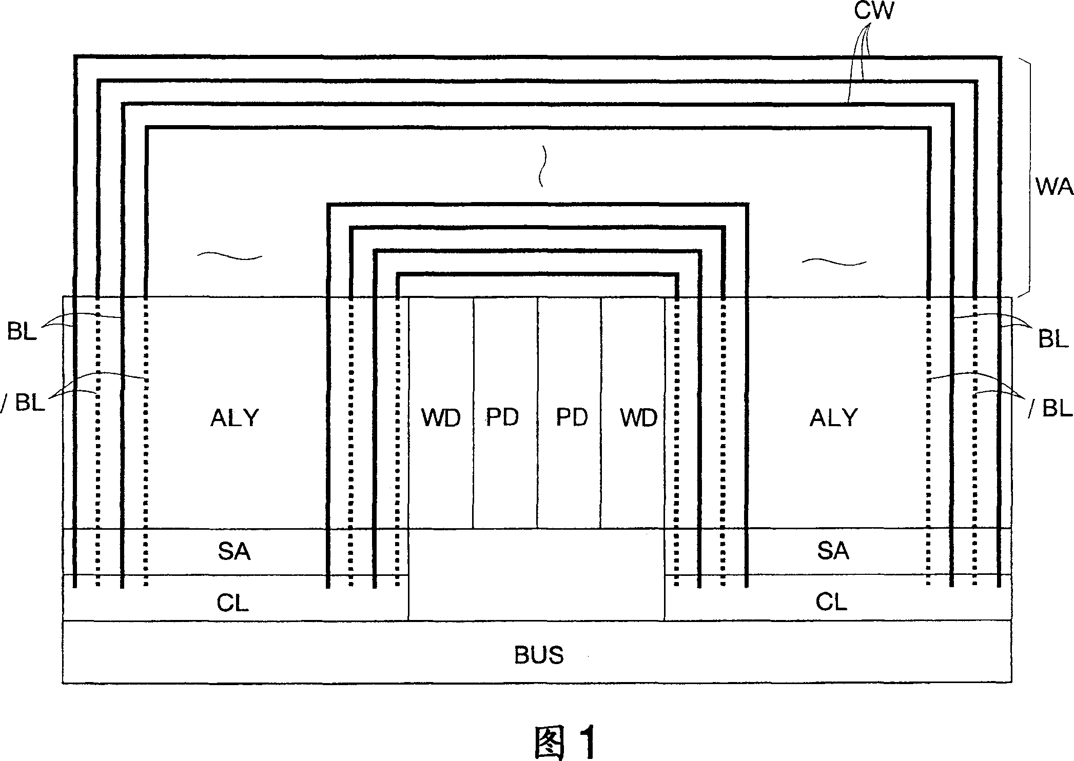
[0040] FIG. 1 shows a first embodiment of a semiconductor memory according to the present invention. This semiconductor memory is formed as a ferroelectric memory on a silicon substrate using a CMOS process. This ferroelectric memory has a storage capacity of 2k bits and can be used as, for example, an authentication chip mounted on an IC card.

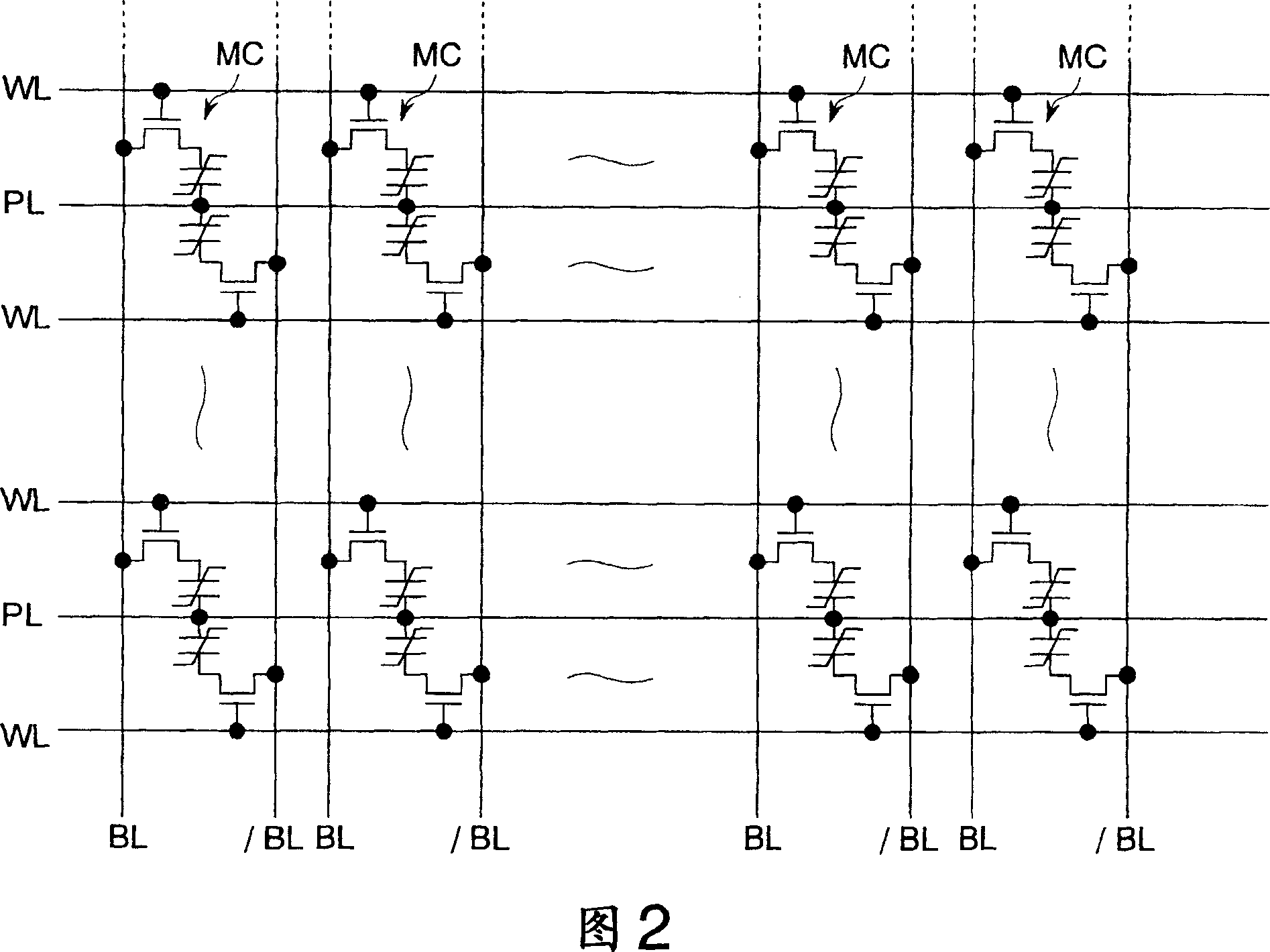
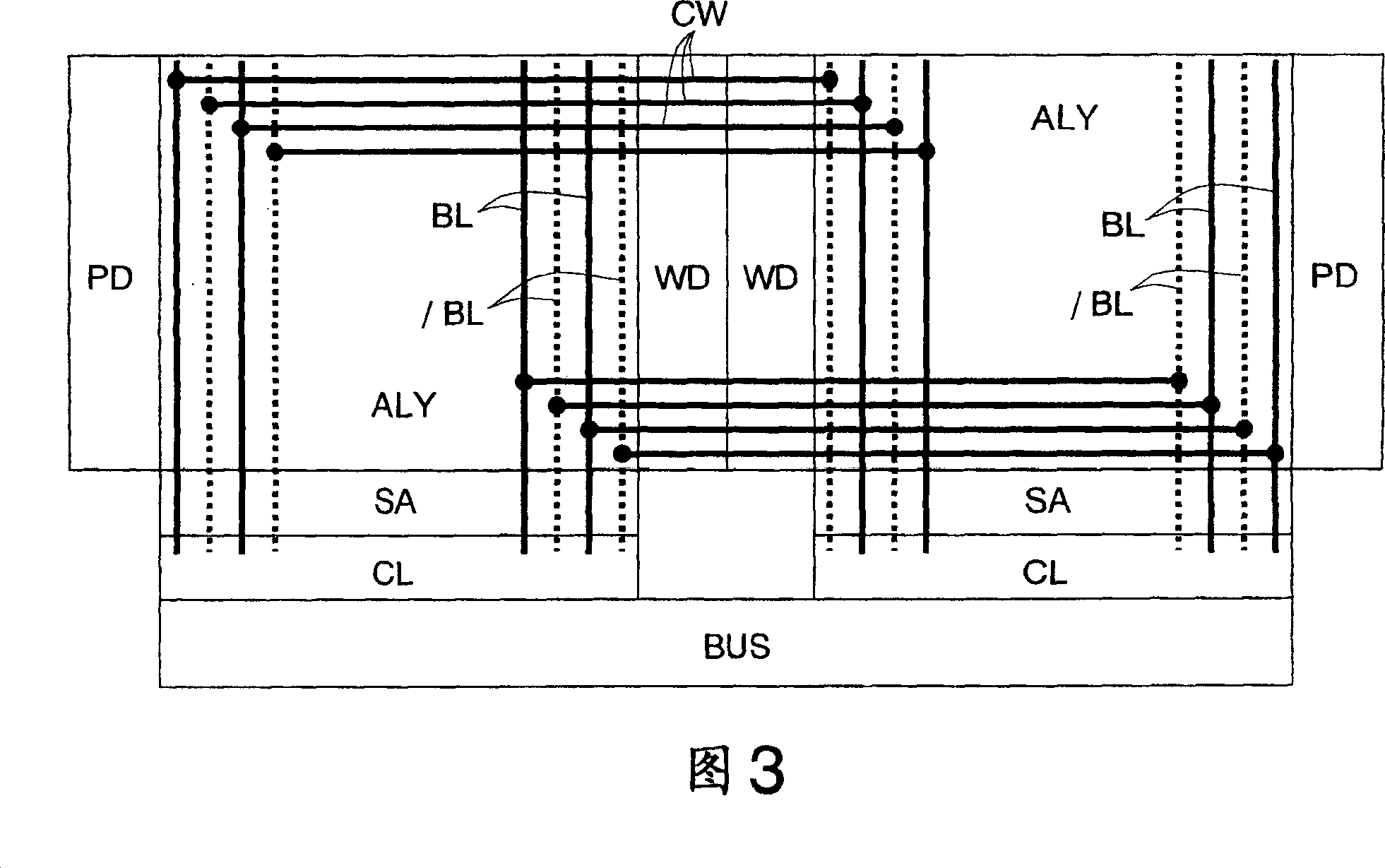
[0041] The ferroelectric memory has two memory cell arrays ALY; the connection leads CW that connect the bit lines BL and / BL of one memory cell array ALY to the respective bit lines of the other memory cell array ALY; Word drive lines WD; plate drive lines PD also associated with respective memory cell arrays ALY; sense amplifiers SA also associated with respective memory cell arrays ALY; column switches CL also associated with respective memory cell arrays ALY; and data Bus BUS.

[0042] The wiring area WA c...


PUM


Abstract

A semiconductor memory is provided that comprises a plurality of memory cell arrays (ALY), each memory cell array (ALY) including bit lines (BL, / BL) and memory cells each constituted by a variable capacitor, the memory cell arrays (ALY) operating at mutually different timings. The bit lines (BL, / BL) of each memory cell array (ALY) are connected to bit lines (BL, / BL) of the other memory cell arrays (ALY) via connecting wires (CW). Accordingly, the actual capacitances of the bit lines (BL, / BL) are the capacitances of bit lines (BL, / BL) of that memory cell array (ALY) itself plus that of the other memory cell arrays (ALY) plus the capacitances of the connecting wires (CW). Therefore, when data is read from the memory cells, the variations in voltage of the bit lines (BL, / BL) caused by the capacitive division can be enlarged. Consequently, the read margin can be prevented from being degraded, and the manufacturing yield of semiconductor memories can be prevented from being degraded. Additionally, since the variations in voltage of the bit lines are enlarged, the data reading time can be shortened.

Description

technical field [0001] The present invention relates to a technique for reliably reading out data from a semiconductor memory in which variable capacitors form individual memory cells. Background technique [0002] Recently, a ferroelectric memory has been developed as a non-volatile semiconductor memory having both the high-speed performance of a DRAM and a flash memory and an EEPROM. For example, each memory cell of a ferroelectric memory has a ferroelectric capacitor and a transfer transistor connecting one end of the ferroelectric capacitor to a bit line. The other end of the ferroelectric memory is connected to a plate line. By making the ferroelectric memory behave like a variable capacitor and taking advantage of the fact that the residual ferroelectric polarization is maintained even if the voltage applied to the ferroelectric capacitor goes to zero, the ferroelectric memory Still able to hold the data. [0003] A read operation of a ferroelectric memory is perfor...

Claims


Application Information

Patent Timeline
Patent Type & Authority Patents(China)
IPC IPC(8): H01L27/10G11C11/34G11C11/22H01L21/8246H01L27/105
CPCG11C11/22
Inventor 野呂幸一
Owner FUJITSU MICROELECTRONICS LTD
Why Eureka
Try Eureka