Supercharge Your Innovation With Domain-Expert AI Agents!

Initial array substrate and manufacturing method and detection method thereof

A manufacturing method and array substrate technology, applied in semiconductor/solid-state device manufacturing, semiconductor/solid-state device testing/measurement, electrical components, etc., can solve problems such as shortened life of display panels

Pending Publication Date: 2020-11-20
BOE TECH GRP CO LTD +1
View PDF0 Cites 2 Cited by
  • Summary
  • Abstract
  • Description
  • Claims
  • Application Information

AI Technical Summary

Problems solved by technology

However, punching holes in the screen will cause oxygen, water vapor, etc. to be absorbed by the organic film layer with better water absorption, which will shorten the life of the display panel.

Method used


Image

  • Initial array substrate and manufacturing method and detection method thereof
  • Initial array substrate and manufacturing method and detection method thereof
  • Initial array substrate and manufacturing method and detection method thereof

Examples


Embodiment

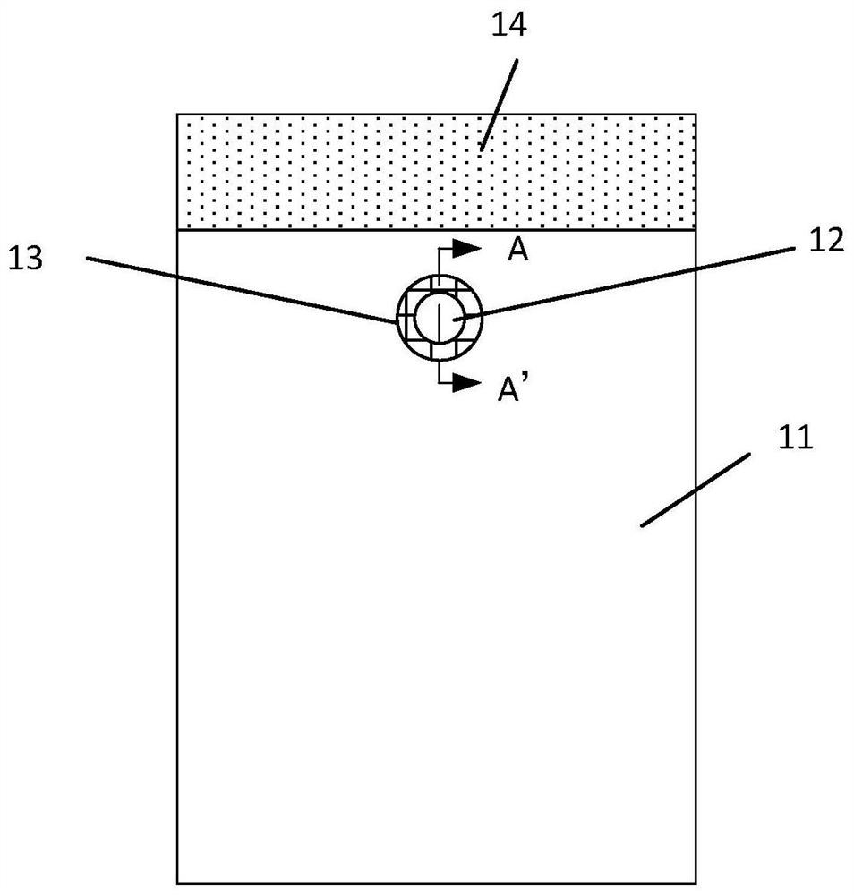
[0127] In this embodiment, the first test conductive pattern RS_1, the second test conductive pattern RS_2, the third test conductive pattern RS_3, the first test conductive pattern RS_1, the second test conductive pattern RS_2 are set in the test conductive layer of the detection area. , The position distribution of the third test conductive pattern RS_3 is as follows Figure 9As shown, wherein the first test conductive pattern RS_1, the second test conductive pattern RS_2, and the third test conductive pattern RS_3 have the same shape. As an optional implementation, the first test conductive pattern RS_1, the second test conductive pattern RS_2, and the third test conductive pattern RS_3 are made as wire windings, and the first test conductive pattern RS_1, the second test conductive pattern RS_2, the third test conductive pattern The wire winding pattern of the third test conductive pattern RS_3, the length and cross-sectional area of ​​the wire winding are equal, and RS_1 ...


PUM


Abstract

The embodiment of the invention provides a manufacturing method for an initial array substrate, and the method comprises the steps: providing an initial substrate which comprises a display region, a hole region, an isolation region and a detection region, enabling the detection region to be located at the periphery of the display region, and enabling the isolation region to be arranged around thehole region; forming an isolation column transition pattern layer in the isolation region, wherein the isolation column transition pattern layer comprises at least one transition isolation column; forming a test conductive layer in the detection region, wherein the test conductive layer comprises a first test conductive pattern and a second test conductive pattern, and the shape of the first testconductive pattern is the same as that of the second test conductive pattern; forming an insulation shielding layer, wherein the insulation shielding layer covers the second test conductive pattern; and etching the initial substrate on which the insulating shielding layer is formed, so that the transition isolation column is etched to form an isolation column, and the cross sectional area of the middle part of the isolation column is smaller than the cross sectional areas of the top and the bottom of the isolation column. The embodiment of the invention further provides an initial array substrate and a detection method of the initial array substrate.

Description

technical field [0001] Embodiments of the present disclosure relate to the field of display technology, and in particular, to a method for manufacturing an initial array substrate, an initial array substrate, and a detection method for an initial array substrate. Background technique [0002] A full screen refers to a display screen with an ultra-high screen-to-body ratio, and an ideal full screen has a screen-to-body ratio of 100%. In order to achieve a full screen, it is necessary to punch holes in a certain position in the screen to install components such as cameras, earpieces, and sensors. However, punching holes in the screen will cause oxygen, water vapor, etc. to be absorbed by the organic film layer with better water absorption, which will shorten the life of the display panel. [0003] In the prior art, isolation columns are often arranged between the opening position and the display area of ​​the display panel, so as to prevent oxygen, water vapor, etc. from bein...

Claims


Application Information

Patent Timeline
IPC IPC(8): H01L21/77H01L27/12H01L21/66H01L23/544
CPCH01L27/1262H01L27/1218H01L22/32H01L22/14H01L22/20
Inventor 刘文慧闫娟李保生吴军李凯鑫
Owner BOE TECH GRP CO LTD
Features
  • R&D
  • Intellectual Property
  • Life Sciences
  • Materials
  • Tech Scout
  • Unparalleled Data Quality
  • Higher Quality Content
  • 60% Fewer Hallucinations
Learn More