PCB element positioning method based on soldering point color distribution

A color distribution and positioning method technology, applied in image analysis, computer parts, image data processing, etc., can solve problems such as low efficiency and cumbersome positioning methods, and achieve the effect of accurately determining the position

Pending Publication Date: 2020-12-04
FOSHAN NANHAI GUANGDONG TECH UNIV CNC EQUIP COOP INNOVATION INST +1
View PDF0 Cites 2 Cited by
  • Summary
  • Abstract
  • Description
  • Claims
  • Application Information

AI Technical Summary

Problems solved by technology

The whole positioning method is cumbersome and inefficient

Method used


Image

  • PCB element positioning method based on soldering point color distribution
  • PCB element positioning method based on soldering point color distribution
  • PCB element positioning method based on soldering point color distribution

Examples


Embodiment Construction

[0051] Below, in conjunction with accompanying drawing and specific embodiment, the present invention is described further:

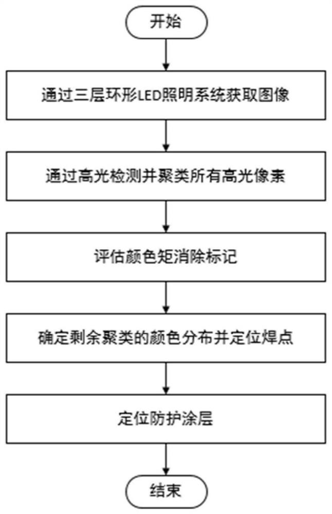
[0052] as attached figure 1 As shown, a kind of PCB component positioning method based on solder joint color distribution provided by the present invention comprises the following steps:

[0053] S01: Acquire the image of the PCB circuit board, extract the high-light pixels in the image, and cluster the high-light pixels according to the distance to form a high-light cluster; wherein, in the present invention, the PCB circuit board image is obtained through a three-layer ring LED lighting system. Specifically include:

[0054] S011: reduce the brightness and contrast of the image; preprocess the image and reduce the brightness and contrast of the image by the following formula:

[0055]p'=[(p+(b+100)×1.27)-127]×[(c+100)×0.01]+127 (1)

[0056] where p is the original pixel, the brightness coefficient b∈(-100, 100), and the contrast coefficient c∈(0, 1...


PUM


Abstract

The invention discloses a PCB element positioning method based on soldering point color distribution, and the method comprises the following steps: S01, obtaining an image of a PCB, extracting highlight pixels in the image, and clustering the highlight pixels according to distances to form highlight clusters; S02, selecting marks from the image to form a mark clustering template, separately calculating the color moment of the highlight pixels in each highlight cluster and the color moment of the marks in the mark clustering template, and determining and removing a mark cluster by determining the difference between the highlight pixel color moment in the highlight cluster and the mark pixel color moment in the mark clustering template; S03, determining soldering point positions according toa fitting result of the color distribution curve of the highlight clusters; and S04, determining the position of a protective coating according to the positions of the soldering points. According tothe method, PCB element positioning can be carried out rapidly and accurately.

Description

technical field [0001] The invention relates to the technical field of detection equipment, in particular to a method for positioning PCB components based on the color distribution of solder joints. Background technique [0002] The demands of the modern manufacturing environment, especially in electronics mass production manufacturing facilities, require that the importance of inspection be magnified. One of the challenges of PCB inspection is when using surface mount device (SMD) placement inspection. Among the many different inspection methods developed, the histogram based method is widely used for PCB component positioning, which is achieved by using x / y projection and threshold to segment the welding area, it is suitable for the local area where the solder joints are concentrated, and the method of only using the histogram is not suitable for the entire complex PCB. [0003] Another typical component localization technique is based on template matching methods. A majo...

Claims


Application Information

Patent Timeline
Patent Type & Authority Applications(China)
IPC IPC(8): G06K9/62G06T5/40G06T7/00G06T7/90
CPCG06T7/0004G06T7/90G06T5/40G06T2207/30148G06F18/23
Inventor 王华龙杨海东宋秋云
Owner FOSHAN NANHAI GUANGDONG TECH UNIV CNC EQUIP COOP INNOVATION INST
Why Eureka
Try Eureka