Pixel circuit, driving method thereof, display panel and display device

A technology of a pixel circuit and a driving module, which is applied in the fields of pixel circuits, display panels and display devices, can solve the problems of short data charging time and the like

Pending Publication Date: 2020-12-04
BOE TECH GRP CO LTD +1
View PDF7 Cites 2 Cited by
  • Summary
  • Abstract
  • Description
  • Claims
  • Application Information

AI Technical Summary

Problems solved by technology

However, displaying a black image between display frames requires twice the video frame rate, which results in less data charging time within each display frame

Method used


Image

  • Pixel circuit, driving method thereof, display panel and display device
  • Pixel circuit, driving method thereof, display panel and display device
  • Pixel circuit, driving method thereof, display panel and display device

Examples


Embodiment 1

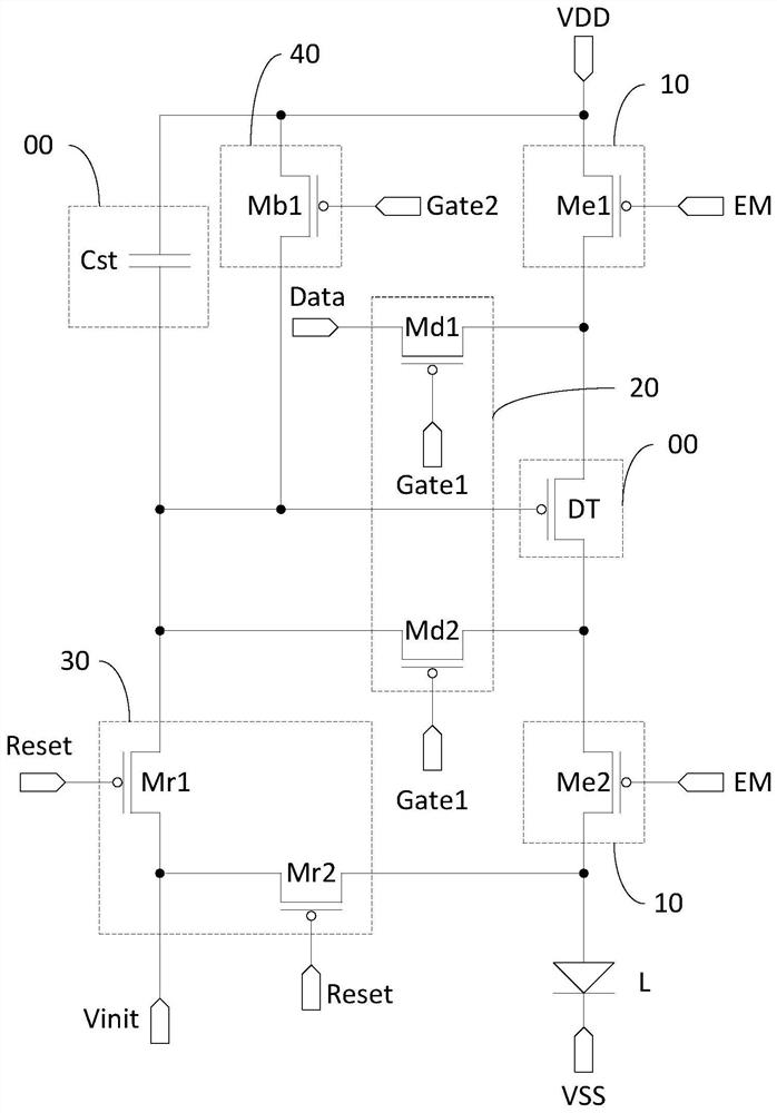
[0099] Below to Figure 5 shown on the display panel, as figure 1 The structure of the pixel circuit shown as an example, combined with Figure 7 The shown signal sequence diagram describes the working process of the above-mentioned display panel provided by the embodiment of the present invention. Among them, RE-n in the figure is the signal of the reset signal terminal Reset of the nth row of subpixels, Gate1-n is the signal of the first scanning signal terminal Gate1 of the nth row of subpixels, and Gate2-n is the signal of the nth row of subpixels The signal of the second scanning signal terminal Gate2, EM-n is the signal of the light emission control signal terminal EM of the nth row of sub-pixels. The working process of the first row of sub-pixels in the display panel is taken as an example for illustration below, and the working process of other rows of sub-pixels in the display panel may be basically the same as that of the first row of sub-pixels. Specifically, cho...

Embodiment 2

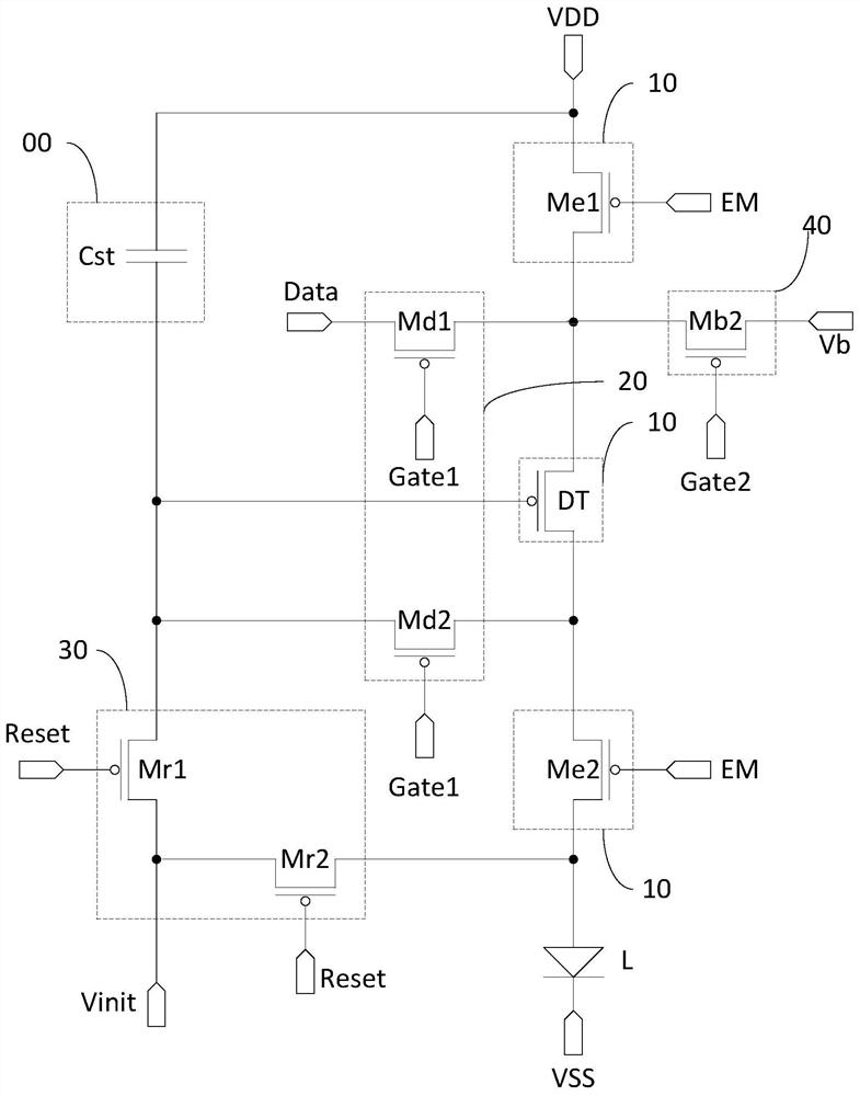
[0109] Below to Figure 5 shown on the display panel, as figure 2 The structure of the pixel circuit shown as an example, combined with Figure 7 The shown signal sequence diagram describes the working process of the above-mentioned display panel provided by the embodiment of the present invention. This embodiment is a modification of some of the implementation manners in the first embodiment. The following only describes the differences between this embodiment and the first embodiment, and the similarities will not be repeated here.

[0110] In the reset phase t1, the data writing phase t2, and the light emitting phase t3, Gate2-1=1, then the second black frame transistor Mb2 is turned off.

[0111]In the black picture insertion stage t4, RE-1=1, Gate1-1=1, Gate2-1=0, EM-1=0. If RE-1=1, the first reset transistor Mr1 and the second reset transistor Mr2 are turned off. Gate1-1=1, then the first data writing transistor Md1 and the second data writing transistor Md2 are tu...

Embodiment 3

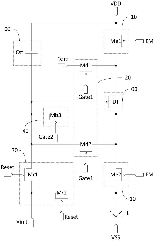
[0113] Below to Figure 5 shown on the display panel, as image 3 The structure of the pixel circuit shown as an example, combined with Figure 7 The shown signal sequence diagram describes the working process of the above-mentioned display panel provided by the embodiment of the present invention. This embodiment is a modification of some of the implementation manners in the first embodiment. The following only describes the differences between this embodiment and the first embodiment, and the similarities will not be repeated here.

[0114] In the reset phase t1, the data writing phase t2, and the light emitting phase t3, Gate2-1=1, the third black frame transistor Mb3 is turned off.

[0115] In the black picture insertion stage t4, RE-1=1, Gate1-1=1, Gate2-1=0, EM-1=0. If RE-1=1, the first reset transistor Mr1 and the second reset transistor Mr2 are turned off. Gate1-1=1, then the first data writing transistor Md1 and the second data writing transistor Md2 are turned o...


PUM


Abstract

The invention discloses a pixel circuit, a driving method thereof, a display panel and a display device. A reset module resets a driving module and a light emitting device under the signal control ofa reset signal end; a data writing module writes the signal of the data signal end and the threshold voltage of a driving transistor in the driving module into the grid electrode of the driving transistor under the signal control of a first scanning signal end; a light-emitting control module drives the light-emitting device to emit light under the signal control of a light-emitting control signalend; by arranging a black picture insertion module, after a light-emitting stage in a display frame time period, under the signal control of the second scanning signal end, the driving transistor iscontrolled to be cut off so as to drive the light-emitting device not to emit light, and black pictures can be inserted in the display frame time period; therefore, the purpose of inserting the blackpicture is achieved under the condition that the charging time is ensured, the moving image response time of the display panel is shortened, and the display effect is improved.

Description

technical field [0001] The present invention relates to the field of display technology, in particular to a pixel circuit, a driving method thereof, a display panel and a display device. Background technique [0002] The organic light emitting diode (Organic Light Emitting Diode, OLED) panel has the characteristics of bendability, high contrast ratio, low power consumption, etc., and has received extensive attention. Among them, the pixel circuit is the core technical content of the OLED panel, which has important research significance. Generally, a method of inserting black images between display frames is used to eliminate the image of the previous frame and reduce the response time of the moving image of the organic light-emitting display. However, displaying a black image between display frames requires twice the video frame rate, which results in less data charging time within each display frame. Contents of the invention [0003] Embodiments of the present inventio...

Claims


Application Information

Patent Timeline
Patent Type & Authority Applications(China)
IPC IPC(8): G09G3/3225
CPCG09G3/3225G09G2320/0252
Inventor 冯靖伊
Owner BOE TECH GRP CO LTD
Why Eureka
Try Eureka