Packaging method and packaging structure of bulk acoustic wave resonator

A technology of bulk acoustic wave resonators and packaging methods, which is applied to electrical components, impedance networks, etc., can solve problems such as device reliability risks, high equipment costs, and production line element pollution, so as to avoid adverse effects, reduce difficulty, and ensure performance. Effect

Active Publication Date: 2020-12-04
NINGBO SEMICON INT CORP
View PDF3 Cites 2 Cited by
  • Summary
  • Abstract
  • Description
  • Claims
  • Application Information

AI Technical Summary

Problems solved by technology

[0009] In the packaging process of the above-mentioned bulk acoustic wave resonator, since it is necessary to deposit and etch a silicon dioxide layer on the carrier substrate, and a gold-gold bonding process is required to bond the first cavity 1011 and the second cavity 2001 together , and the carrier substrate needs to be removed after bonding, so the process is complicated and the equipment cost is high
And because the gold-gold bonding process introduces gold elements, there are problems of high material cost and element pollution to the production line
In addition, the passivation layer 205 in the above process is usually formed by depositing a thin layer of commonly used passivation layer materials such as silicon oxide or silicon nitride, which will cause gaps in the hole 203, so that the second cavity 2001 The sidewall is thinner, which leads to insufficient mechanical strength of the upper chamber cover, which will lead to device reliability risks

Method used


Image

  • Packaging method and packaging structure of bulk acoustic wave resonator
  • Packaging method and packaging structure of bulk acoustic wave resonator
  • Packaging method and packaging structure of bulk acoustic wave resonator

Examples


Embodiment Construction

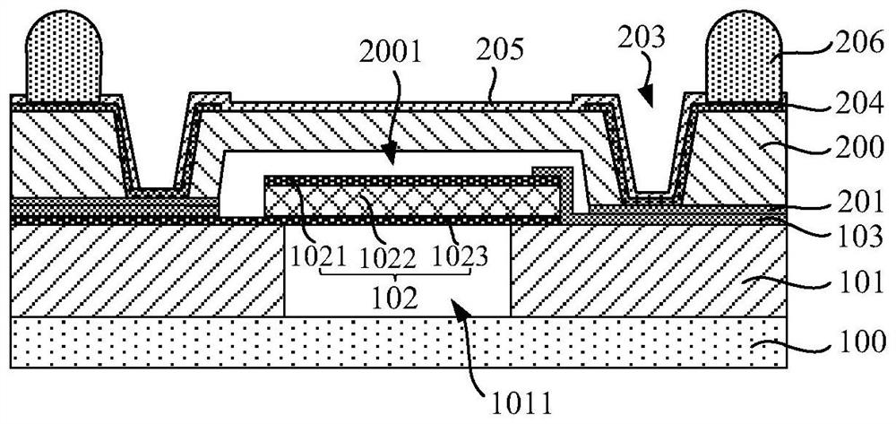
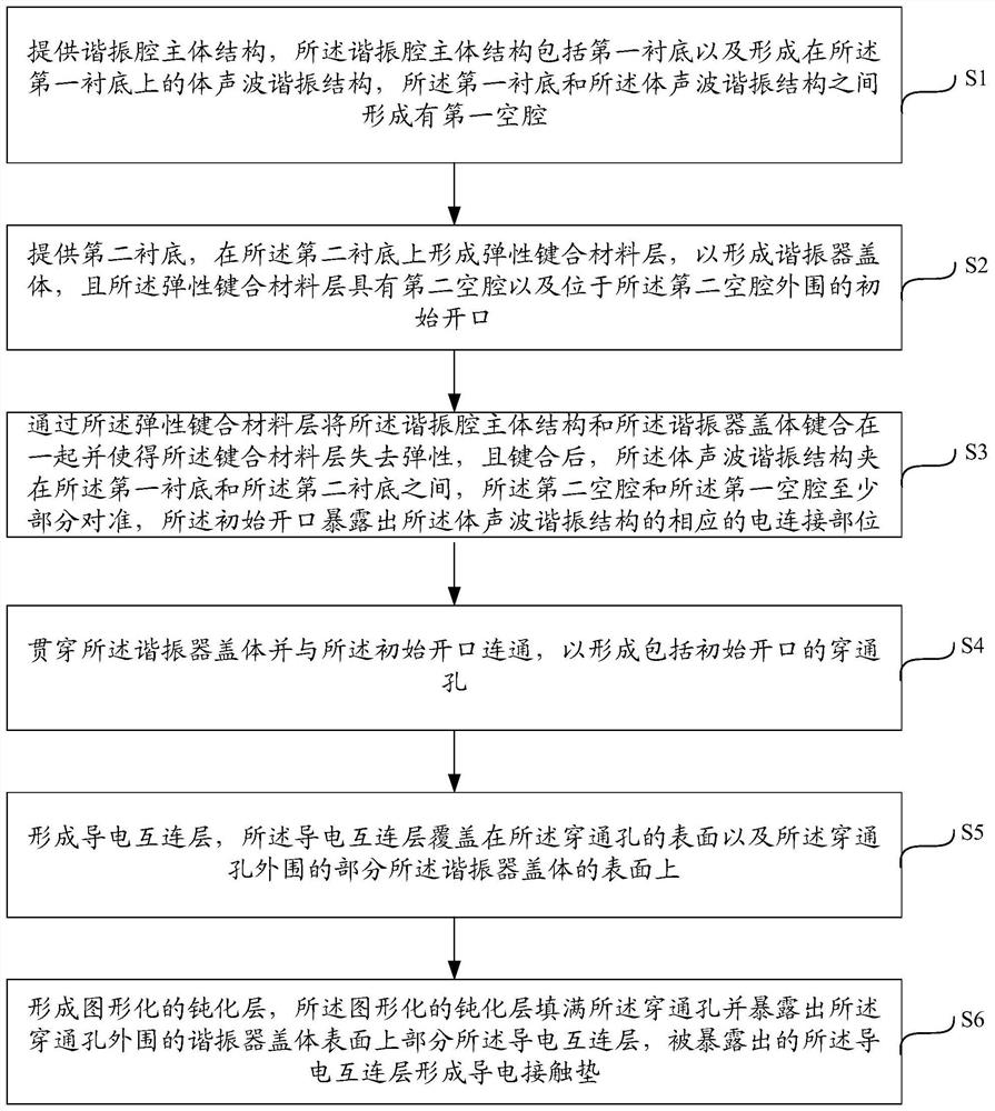
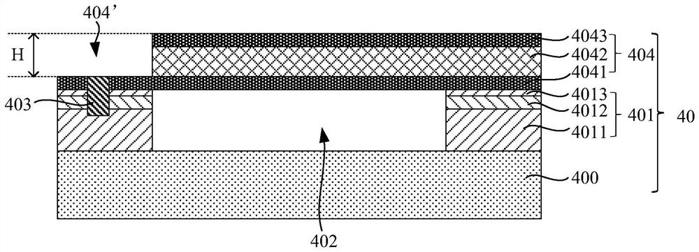
[0032] The technical solutions of the present invention will be described in further detail below in conjunction with the accompanying drawings and specific embodiments. The advantages and features of the present invention will become clearer from the following description. It should be noted that the drawings are all in a very simplified form and use inaccurate scales, and are only used to facilitate and clearly assist the purpose of illustrating the embodiments of the present invention. Similarly, if a method described herein includes a series of steps, the order in which these steps are presented is not necessarily the only order in which these steps can be performed, and some described steps may be omitted and / or some not described herein Additional steps can be added to the method. If the components in a certain drawing are the same as those in other drawings, although these components can be easily identified in all the drawings, in order to make the description of the ...


PUM

PropertyMeasurementUnit
thicknessaaaaaaaaaa
thicknessaaaaaaaaaa
thicknessaaaaaaaaaa

Abstract

The invention provides a packaging method and a packaging structure of a bulk acoustic wave resonator. A resonator cover body is manufactured by forming an elastic bonding material layer with a secondcavity and an initial opening on a second substrate, then the resonator cover body can be directly bonded with a resonant cavity main body structure through the elastic bonding material layer on theresonator cover body, then the resonator cover body can penetrate through the resonator cover body and is communicated with the initial opening to form a through hole, and a conductive interconnectionlayer is formed on the inner surface of the through hole and a part of the surface of the second substrate. Because the initial opening is firstly formed, and then the second substrate is penetratedto be communicated with the initial opening so as to obtain the complete through hole, the difficulty of forming the through hole can be reduced, the adverse effect on the performance of the resonatorcaused by the process of forming the through hole and the conductive interconnection layer can be avoided, the reliability of the resonator is improved, and meanwhile, the performance of the formed through hole and the conductive interconnection layer is ensured.

Description

technical field [0001] The present invention relates to the technical field of packaging of radio frequency products, in particular to a packaging method and packaging structure of a bulk acoustic wave resonator. Background technique [0002] A bulk acoustic resonator (FBAR) includes electrodes typically disposed above and / or below a piezoelectric layer. The piezoelectric layer can oscillate in response to a high frequency signal applied to the electrodes. FBARs can be used in wireless signal transmission systems to enable wireless data input and / or output. For example, FBARs may be used in wireless communication devices, wireless power transmitters, filters for wireless sensors, transmitters, receivers, duplexers, and the like. [0003] Please refer to figure 1 , the current conventional BAW resonator packaging process usually includes the following steps: [0004] (1) A silicon dioxide layer 200 is grown on a carrier substrate (not shown) by a thermal oxidation process...

Claims


Application Information

Patent Timeline
Patent Type & Authority Applications(China)
IPC IPC(8): H03H3/02H03H9/02H03H9/05H03H9/10
CPCH03H3/02H03H9/02015H03H9/02102H03H9/02133H03H9/02047H03H9/0504H03H9/1007H03H2003/023H03H9/174H03H9/1035H03H9/173H03H2003/021
Inventor 罗海龙
Owner NINGBO SEMICON INT CORP
Why Eureka
Try Eureka