Power converter based on dynamic zero compensation circuit
A technology of power converter and dynamic zero point, which is applied in the direction of adjusting electric variable, converting device of output power, converting DC power input to DC power output, etc. It can solve problems such as failure to meet requirements, achieve high practical value, and maintain transient state response, the effect of fast transient response
- Summary
- Abstract
- Description
- Claims
- Application Information
AI Technical Summary
Problems solved by technology
Method used
Image

Examples
Embodiment 1
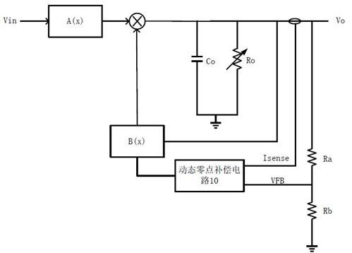
[0057] Specifically, see Figure 5 , the dynamic zero compensation circuit 10 includes an operational amplifier OP1, an operational amplifier OP2, a field effect transistor MN1, a field effect transistor MN2, a field effect transistor MN3, a field effect transistor MN4, a field effect transistor MP1, a field effect transistor MP2, a resistor RM, and a resistor RN , the non-inverting input terminal of the operational amplifier OP1 is connected to the signal Isense, the inverting input terminal of the operational amplifier OP1 is connected to the signal VFB, the output terminal of the operational amplifier OP1 is connected to one end of the resistor RM, the gate of the field effect transistor MN4, and the field effect transistor The gate of MN1 is connected to the other end of the resistor RM and the drain of the field effect transistor MN2, the gate of the field effect transistor MN2 is connected to the gate of the field effect transistor MN3, the gate of the field effect transi...
Embodiment 2
[0078] see Figure 6 , the present embodiment provides another dynamic zero point compensation circuit 10, the dynamic zero point compensation circuit 10 of the present embodiment includes an operational amplifier OP1, an operational amplifier OP2, an operational amplifier OP3, an operational amplifier OP4, a field effect transistor MP1, and a field effect transistor MP2 , FET MP3, FET MP4, FET MN1, FET MN4, resistor RM, resistor RN, resistor RP, the non-inverting input terminal of the operational amplifier OP1 is connected to the signal Isense, and the inverting input terminal of the operational amplifier OP1 The signal VFB is connected, the gate of the field effect transistor MN1 is connected to the output terminal of the operational amplifier OP1 and the non-inverting input terminal of the operational amplifier OP2, and the output terminal of the operational amplifier OP2 is connected to the gate of the field effect transistor MP1 and the gate of the field effect transistor ...
PUM
 Abstract
Description
Claims
Application Information
 - R&D
- Intellectual Property
- Life Sciences
- Materials
- Tech Scout
- Unparalleled Data Quality
- Higher Quality Content
- 60% Fewer Hallucinations
Browse by: Latest US Patents, China's latest patents, Technical Efficacy Thesaurus, Application Domain, Technology Topic, Popular Technical Reports.
© 2025 PatSnap. All rights reserved.Legal|Privacy policy|Modern Slavery Act Transparency Statement|Sitemap|About US| Contact US: help@patsnap.com