PCB detection and review method and device, electronic equipment and storage medium

A detection method and detection point technology, applied in electrical digital data processing, computer-aided design, special data processing applications, etc., can solve the problems of increased average cost of PCB board repair, repeated use of testing equipment, and different detection coverage. Achieve the effect of promoting smooth detection, avoiding repeated detection, and ensuring detectability

Active Publication Date: 2020-12-25
VAYO SHANGHAI TECH
View PDF6 Cites 2 Cited by
  • Summary
  • Abstract
  • Description
  • Claims
  • Application Information

AI Technical Summary

Problems solved by technology

[0007] Previous inspection data show that for a medium-complexity PCB board (about 3000 solder joints and about 500 components), if the defect escapes the current inspection and is discovered in the next inspection, the average cost of PCB board repair will be about Increase by 6 to 7 times, and the loss caused by PCB scrapping will also rise in a straight line
Generally, the one-time yield rate of PCB boards is between 60% and 90%. If it is not strictly tested, it will cause huge waste. If defective products flow into the market, the losses to the enterprise will be immeasurable. Therefore, PCB manufacturers will purchase PCB testing equipment with various testing technologies to test PCBs. Therefore, it is also very important to invest, configure and use expensive PCB testing and testing equipment reasonably to maximize the benefits of the equipment. of
In the industry, there are many detection methods for defects such as missing PCB components, open circuits, short circuits, directions, and wrong materials, but the detection coverage of each detection method is different, and often the same defect is repeatedly detected by multiple detection equipment, which directly leads to The repeated use of testing equipment will indirectly cause the extension of the NPI (New Product Input, new product introduction) cycle, which will bring great losses to the enterprise.

Method used


Image

  • PCB detection and review method and device, electronic equipment and storage medium
  • PCB detection and review method and device, electronic equipment and storage medium
  • PCB detection and review method and device, electronic equipment and storage medium

Examples


Embodiment 1

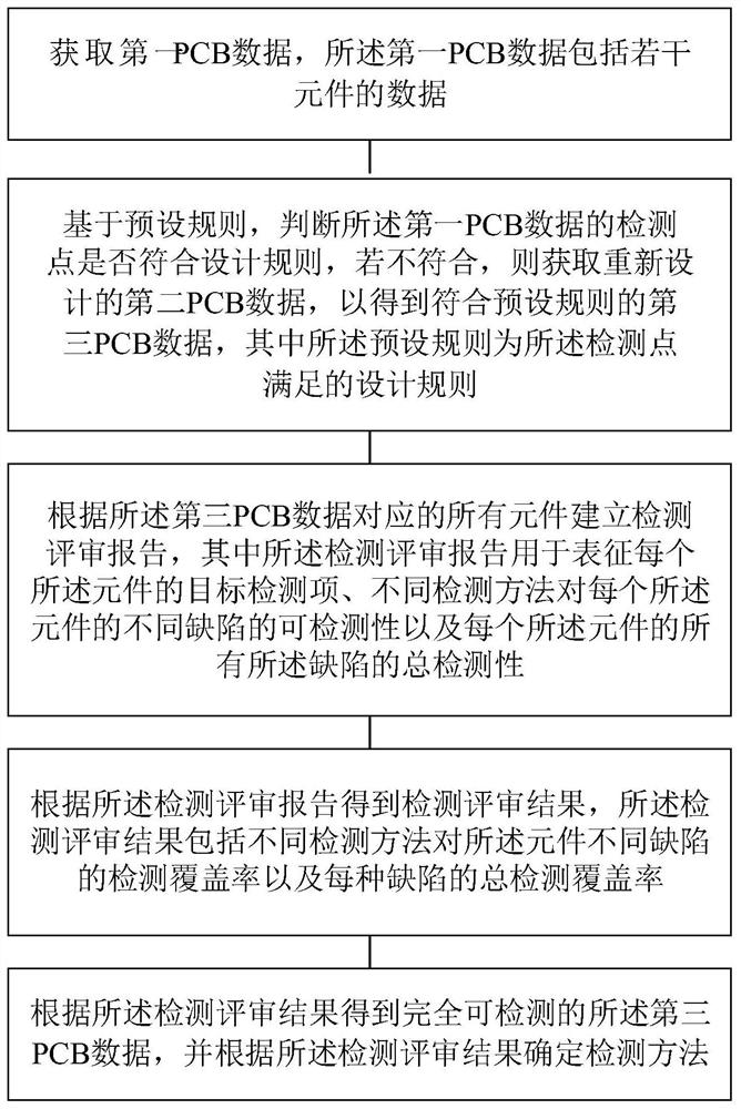
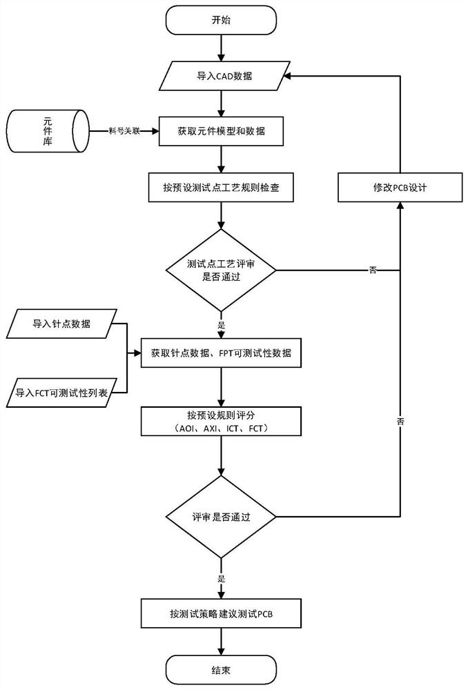
[0061] See figure 1 and figure 2 Understand the technical solution of this embodiment. This embodiment provides a method for PCB inspection and review, which may specifically include:

[0062] Step 1, obtaining the first PCB data, the first PCB data includes the data of several components;

[0063] Step 2. Based on the preset rules, judge whether the detection point of the first PCB data conforms to the design rules, and if not, obtain the redesigned second PCB data to obtain the third PCB data conforming to the preset rules, wherein the preset The rule is the design rule that the detection point satisfies;

[0064] Step 3. Establish a test review report based on all components corresponding to the third PCB data, wherein the test review report is used to characterize the target test items of each component, the detectability of different defects of each component by different detection methods, and the The total detectability of all defects in ;

[0065] Step 4. Obtain ...

Embodiment 2

[0136] See Figure 9 , Figure 9 It is a schematic structural diagram of a PCB inspection and evaluation device provided in this embodiment. The PCB inspection review device includes:

[0137] An acquisition module, configured to acquire first PCB data, where the first PCB data includes data of several components;

[0138] The design module is used to judge whether the detection point of the first PCB data conforms to the design rules based on the preset rules, and if not, obtain the redesigned second PCB data to obtain the third PCB data conforming to the preset rules, wherein The preset rule is the design rule satisfied by the detection point;

[0139] The detection review report building module is used to establish a test review report based on all components corresponding to the third PCB data, wherein the test review report is used to characterize the target detection items of each component, and the detectability of different defects of each component by different det...

Embodiment 3

[0144] See Figure 10 , Figure 10 It is a schematic structural diagram of an electronic device provided in this embodiment. The electronic device 1100 includes: a processor 1101, a communication interface 1102, a memory 1103, and a communication bus 1104, wherein the processor 1101, the communication interface 1102, and the memory 1103 complete mutual communication through the communication bus 1104;

[0145] memory 1103, for storing computer programs;

[0146] The processor 1101 is configured to implement the above method steps when executing the computer program.

[0147] When the processor 1101 executes the computer program, the following steps are implemented:

[0148] Step 1, obtaining the first PCB data, the first PCB data includes the data of several components;

[0149] Step 2. Based on the preset rules, judge whether the detection point of the first PCB data conforms to the design rules, and if not, obtain the redesigned second PCB data to obtain the third PCB data...


PUM


Abstract

The invention discloses a PCB detection review method, a PCB detection review device, electronic equipment and a storage medium. The method comprises the following steps: acquiring first PCB data; based on a preset rule, designing the first PCB data according to the detection points on the first PCB data to obtain third PCB data conforming to the preset rule; establishing a detection review reportaccording to all elements corresponding to the third PCB data; obtaining a detection review result according to the detection review report; and obtaining completely detectable third PCB data according to the detection and review result, and determining a detection method according to the detection and review result. According to the method, repeated detection is avoided while the machine cost issaved, smooth PCB production detection is promoted, the product reliability is guaranteed, the whole NPI period is shortened, and more profits can be created for enterprises.

Description

technical field [0001] The invention belongs to the technical field of printed circuit boards, and in particular relates to a PCB detection and review method, a review device, electronic equipment and a storage medium. Background technique [0002] A qualified PCB (Printed Circuit Board, printed circuit board) should have three major characteristics: manufacturability, detectability, and reliability. The detectability is embodied in the design of PCB inspection points. Only PCBs are qualified products, and only PCB boards with reasonable design of inspection points can pass the inspection, so the evaluation of inspection points is also an important link in PCB manufacturing. [0003] The PCB detection point is a pad specially designed to connect with the contact pin of the detection equipment, and is mainly used to detect the on-off and other parameters of the current circuit. In the industry, as early as the PCB design stage, engineers will complete the circuit design in E...

Claims


Application Information

Patent Timeline
Patent Type & Authority Applications(China)
IPC IPC(8): G06F30/398
CPCG06F30/398Y02P90/30
Inventor 黄越钱胜杰刘华刘丰收
Owner VAYO SHANGHAI TECH
Why Eureka
Try Eureka