Semiconductor ceramic packaging shell

A ceramic packaging and semiconductor technology, which is applied to semiconductor devices, semiconductor/solid-state device components, electric solid-state devices, etc. Into and other problems, to avoid the effect of not easy to deal with

Inactive Publication Date: 2020-12-29
徐梦雪
View PDF0 Cites 0 Cited by
  • Summary
  • Abstract
  • Description
  • Claims
  • Application Information

AI Technical Summary

Problems solved by technology

[0003] Since the semiconductor ceramic package shell can protect the internal chip from external impact, but the impact force that the semiconductor ceramic package shell can withstand is limited, if the semiconductor ceramic package shell used in the stone cutting machine is cracked by the impact of tiny stones entering the heat dissipation port , it is easy to generate debris on the inner wall of the ceramic after being impacted again and fall into the circuit connection between the chip and the semiconductor ceramic package shell, resulting in a decrease in the transmission efficiency between the chip and the semiconductor ceramic package shell

Method used


Image

  • Semiconductor ceramic packaging shell
  • Semiconductor ceramic packaging shell
  • Semiconductor ceramic packaging shell

Examples


Embodiment 1

[0026] For example figure 1 -example Figure 5 Shown:

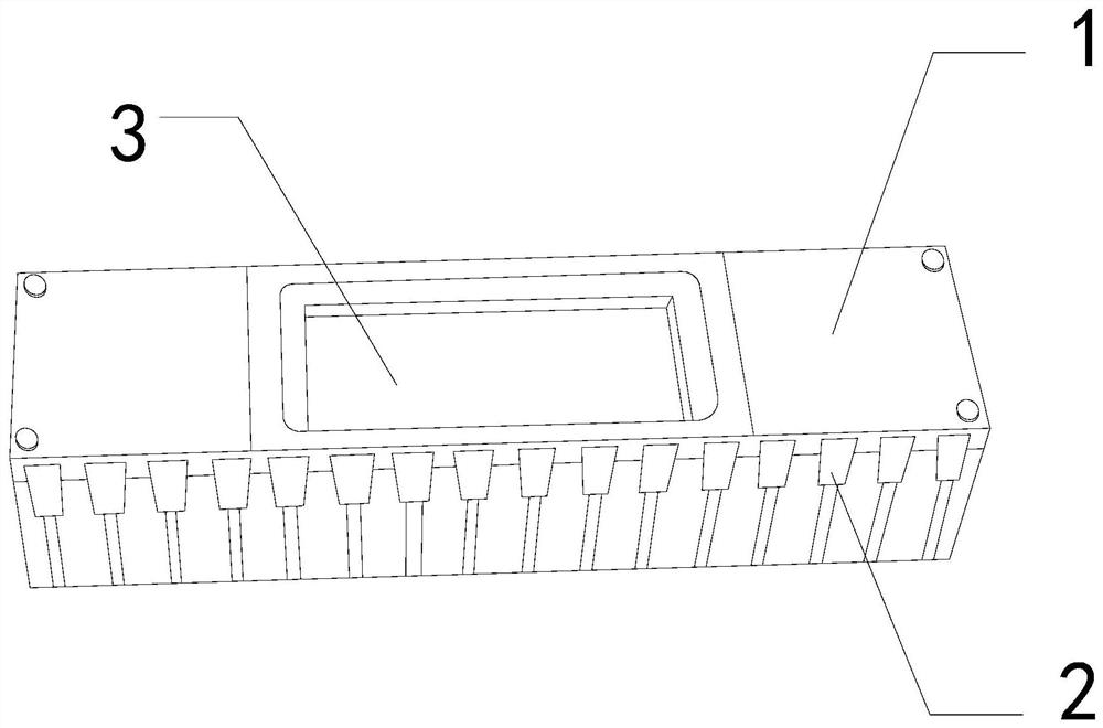
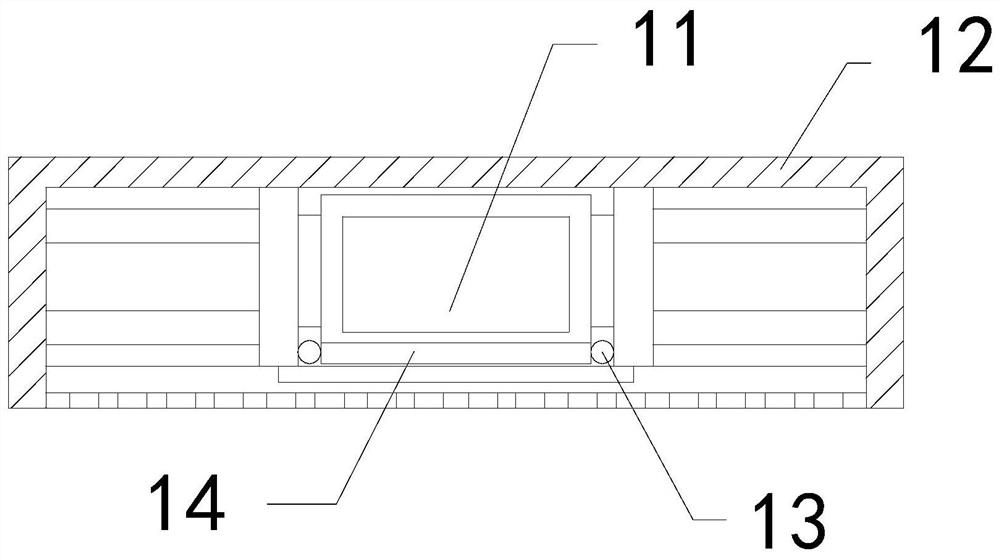
[0027] The present invention provides a semiconductor ceramic packaging shell, the structure of which includes a protective shell 1, an electrical terminal 2, and a chip cavity 3, the electrical terminal 2 is embedded in the front end of the protective shell 1, and the protective shell 1 and the chip cavity 3 is an integrated structure; the protective shell 1 includes a chip 11, a shell 12, a movable ball 13, and a contact plate 14, the chip 11 is embedded in the inner center of the shell 12, and the movable ball 13 is installed between the chip 11 and the contact plate 14. Between the inner walls of the housing 12 , the contact plate 14 and the chip 11 are integrated.

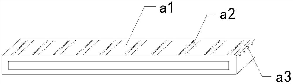
[0028] Wherein, the contact plate 14 includes a plate body a1, a concentration groove a2, and an outer row hole a3, the concentration groove a2 is embedded in the upper surface of the plate body a1, and the outer row hole a3 and the plate body a1 are an...

Embodiment 2

[0034] For example Image 6 -example Figure 8 Shown:

[0035] Wherein, the movable ball 13 includes an outer contact ring c1, a guide mechanism c2, a middle solid block c3, and a collection groove c4. The outer contact ring c1 is movably engaged with the middle solid block c3. c1 is an integrated structure, the collection groove c4 is embedded and connected with the middle solid block c3, the guide mechanism c2 is provided with four, and is evenly distributed in a circle on the outer contact ring c1, and the outer contact ring c2 can be guided by the guide mechanism c2 The ceramic debris is introduced between the outer contact ring c1 and the middle solid block c3.

[0036] Wherein, the guide mechanism c2 includes a fitting block c21, an outer sliding plate c22, an elastic strip c23, and a frame c24. The fitting block c21 is embedded and fixed at the front end of the outer sliding plate c22, and the elastic strip c23 is installed on the outer sliding plate c22. Between the...


PUM


Abstract

The invention discloses a semiconductor ceramic packaging shell which structurally comprises a protective shell, a power connection end and a chip cavity. The power connection end is fixedly embeddedin the front end of the protective shell, the protective shell and the chip cavity are an integrated structure, and when a transition plate slides downwards to the maximum extent, the bottom of a bottom plate is impacted by the transition plate so that an upper swing plate can be reversely pushed by a vibration force to swing upwards, ceramic chippings on the upper surface of the upper swing platecan be guided into a chip removal cavity in cooperation with vibration balls rolling from inner walls towards the two sides, and the ceramic chippings can be gradually discharged outwards along withvibration generated in the operation process of the cutting machine through the chip removal cavity along with the outer discharge holes. Through vibration generated during operation of the cutting machine, an outer sliding plate on the guide mechanism can extend outwards along the frame so that ceramic chips guided out from the interior of the outer discharge holes can be guided into the collecting groove in a middle fixing block through the guide mechanism, and then the ceramic chips on the outer surface can be gradually guided into the inner portion through a blocking cavity.

Description

technical field [0001] The invention relates to the field of conductor ceramics, in particular to a semiconductor ceramic package shell. Background technique [0002] The semiconductor ceramic packaging shell is mainly used for packaging small-scale container chips. The semiconductor ceramic package shells on both sides wrap the chip, so as to protect the chip and enhance the transmission efficiency. Based on the above Description The inventors have found that an existing semiconductor ceramic packaging shell mainly has the following deficiencies, for example: [0003] Since the semiconductor ceramic package shell can protect the internal chip from external impact, but the impact force that the semiconductor ceramic package shell can withstand is limited, if the semiconductor ceramic package shell used in the stone cutting machine is cracked by the impact of tiny stones entering the heat dissipation port , it is easy to generate debris on the inner wall of the ceramic after...

Claims


Application Information

Patent Timeline
Patent Type & Authority Applications(China)
IPC IPC(8): H01L23/04H01L23/06H01L23/10
CPCH01L23/04H01L23/06H01L23/10
Inventor 徐梦雪
Owner 徐梦雪
Why Eureka
Try Eureka