
Voltage-sensitive ceramic interface state response measurement method based on frequency domain dielectric response

A varistor ceramics, dielectric response technology, applied in measuring devices, measuring electrical variables, measuring resistance/reactance/impedance, etc., can solve the problem that the interface state response cannot disappear immediately

Active Publication Date: 2021-01-05
XI AN JIAOTONG UNIV
View PDF8 Cites 3 Cited by
  • Summary
  • Abstract
  • Description
  • Claims
  • Application Information

AI Technical Summary

Problems solved by technology

However, after the DC bias is removed, the interface state response cannot disappear immediately, and it takes a certain amount of time

Method used


Image

  • Voltage-sensitive ceramic interface state response measurement method based on frequency domain dielectric response
  • Voltage-sensitive ceramic interface state response measurement method based on frequency domain dielectric response
  • Voltage-sensitive ceramic interface state response measurement method based on frequency domain dielectric response

Examples


Embodiment 1

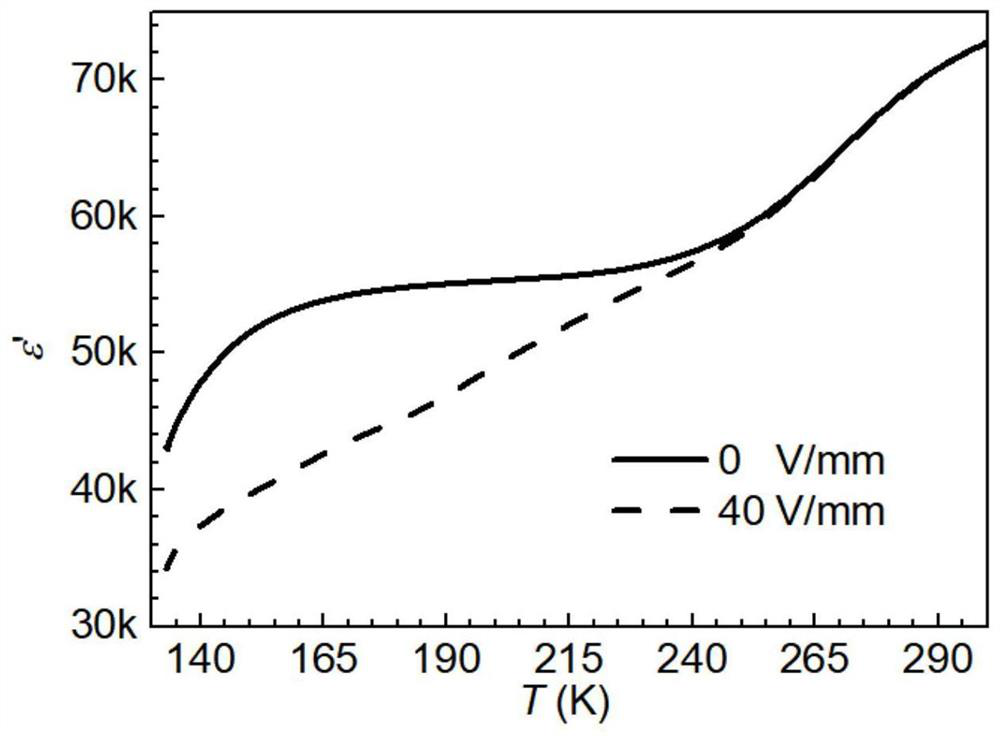
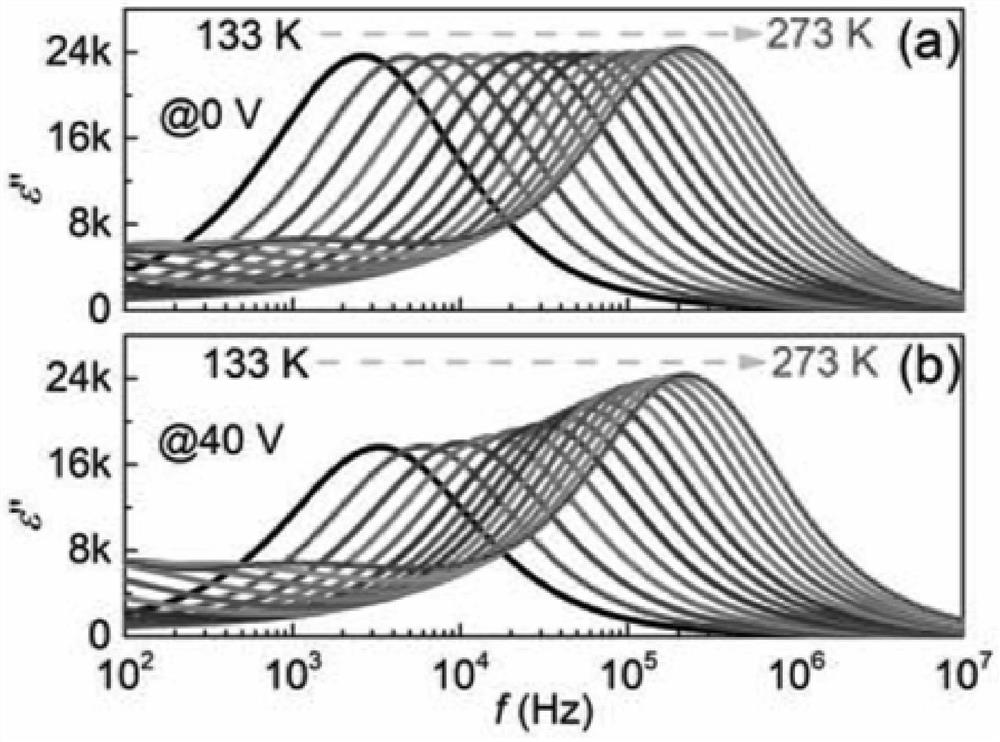
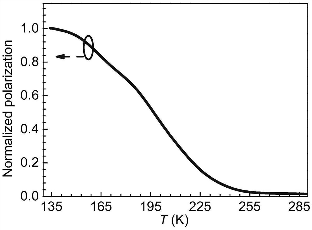
[0036] with CaCu 3 Ti 4 O 12 (CCTO) ceramics as an example, the sample was pretreated at a temperature of 50 °C for 24 h to release various stress histories inside the sample. With the help of a liquid nitrogen cooling system, the temperature of the sample was lowered to -140 °C and the temperature was kept stable. First, set the DC bias voltage so that the electric field strength of the sample is 0V / mm and maintain it for 3min, then measure the frequency domain dielectric spectrum of the sample under the AC signal of 1V. Then, the sample was heated to 30°C at a heating rate of 3°C / min, and the frequency domain dielectric spectrum of the sample under AC small signal was measured at every 0.2°C temperature during the heating process. Next, cool the sample from 30°C to -140°C, apply a DC bias voltage across the sample to make the electric field strength of the sample 40V / mm and maintain it for 3min, then heat the sample at a heating rate of 3°C / min , the sample was heated fr...


PUM


Abstract

The invention discloses a voltage-sensitive ceramic interface state response measurement method based on frequency domain dielectric response. The method comprises the steps of 1) heating or cooling asample to an initial test temperature, setting a direct current bias voltage to enable the electric field intensity of the sample to be 0V / mm, keeping the electric field intensity for a first set time, removing the direct current bias voltage, measuring the frequency domain dielectric spectrum of the sample under a set alternating current signal, heating according to a set heating rate, continuously measuring the frequency domain dielectric spectrum of the sample until the temperature of the sample reaches a preset test ending temperature, and obtaining a first frequency domain dielectric spectrum of the sample; 2) repeating the step 1) to modulate the electric field intensity to n V / mm to obtain a second frequency domain dielectric spectrum of the sample; and 3) subtracting the first frequency domain dielectric spectrum from the second frequency domain dielectric spectrum to obtain a voltage-sensitive ceramic interface state response curve, wherein n is less than the breakdown fieldintensity of the sample. The test result can well represent the characteristics of the interface state response of the sample. The method is an effective method for testing the interface state response of a back-to-back barrier.

Description

technical field [0001] The invention belongs to the field of semiconductor ceramics, and particularly relates to a method for measuring the interface state response of pressure-sensitive ceramics based on the dielectric response in the frequency domain. Background technique [0002] Among many functional ceramic materials, the back-to-back Schottky barrier at the grain boundary is the origin of its functionalization, which determines the short-term functional properties and stability of the ceramic dielectric. In general, this back-to-back Schottky barrier consists of two parts: negatively charged interface state defects at grain boundaries and a depletion layer at the grain surface. The characterization and detection of the defect response in the depletion layer has been relatively mature, but there are still questions about how to detect the interface state defect structure response characteristics. [0003] The characteristics of the dynamic response of the interface sta...

Claims


Application Information

Patent Timeline
Patent Type & Authority Applications(China)
IPC IPC(8): G01R27/26
CPCG01R27/2623
Inventor 武康宁李建英王瑶侯宗克郭璊李盛涛
Owner XI AN JIAOTONG UNIV
Learn More