
Display device and electronic equipment

A display device and main display technology, which is applied in the direction of circuits, electrical components, electric solid devices, etc., can solve the problem of uneven display in the main display area, and achieve the effect of avoiding uneven display and simplifying wiring design

Pending Publication Date: 2021-01-22
WUHAN CHINA STAR OPTOELECTRONICS SEMICON DISPLAY TECH CO LTD
View PDF1 Cites 2 Cited by
  • Summary
  • Abstract
  • Description
  • Claims
  • Application Information

AI Technical Summary

Problems solved by technology

[0005] The purpose of this application is to provide a display device and electronic equipment, which can improve the problem of uneven display in the main display area of ​​the display device and electronic equipment with a display light transmission area, and simplify the connection of the first signal line around the display light transmission area. Wiring method to simplify the process

Method used


Image

  • Display device and electronic equipment
  • Display device and electronic equipment
  • Display device and electronic equipment

Examples


Embodiment Construction

[0044] The technical solutions in the embodiments of the present application will be clearly and completely described below in conjunction with the drawings in the embodiments of the present application. Apparently, the described embodiments are only some of the embodiments of this application, not all of them. Based on the embodiments in this application, all other embodiments obtained by those skilled in the art without making creative efforts belong to the scope of protection of this application.

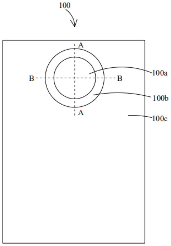
[0045] The present application provides a display device, and the display device 100 may be a liquid crystal display device or an organic light emitting diode display device. Specifically, the display device 100 is an OLED display device.

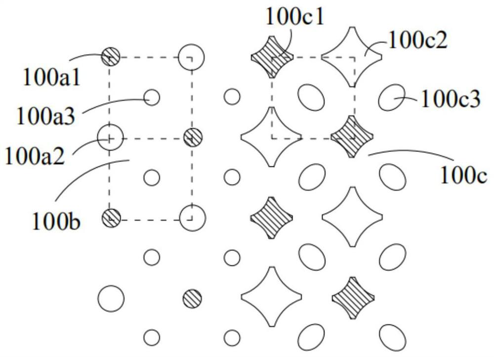
[0046] see figure 1 and figure 2 as shown, figure 1 is a schematic plan view of a display device according to an embodiment of the present application, figure 2 for figure 1 A schematic diagram of the distribution of the first display pi...


PUM


Abstract

The invention provides a display device and electronic equipment, the display device is provided with a display light-transmitting area, a main display area and a transition display area, the transition display area is arranged between the display light-transmitting area and the main display area, and the display device comprises a plurality of first display pixels arranged in the main display area; a plurality of second display pixels which are arranged in the display light-transmitting area and the transition display area; a plurality of pixel driving circuit islands which are arranged in the transition display area and distributed around the display light-transmitting area; a plurality of first signal lines, wherein each of the first signal lines comprises a connecting section, and theconnecting sections of the first signal lines are arranged between the pixel driving circuit islands and the display area light-transmitting area and are connected with the pixel driving circuit islands. According to the display device, the connecting sections of the first signal lines are arranged between the pixel driving circuit islands and the display light-transmitting area, so that the wiring mode when the connecting sections of the first signal lines are connected with the corresponding pixel driving circuit islands is simplified, the problem of uneven display of the display device is solved, and the display effect of the electronic equipment is improved.

Description

technical field [0001] The present application relates to the field of display technology, in particular to a display device and electronic equipment. Background technique [0002] At present, it is one of the research hotspots to adopt a transparent display design for the under-screen camera area of ​​the Active Metrix Organic Light Emitting Diode (AMOLED) display panel to realize a full-screen design. [0003] In the Chinese patent application with publication number CN110491917A proposed by the applicant, the pixel drive circuit island and the first signal line and the second signal line electrically connected to multiple pixel drive circuit islands are arranged outside the light transmission area to increase light transmission. area transmittance. However, the applicant found that the wiring method of the second detour sections of the plurality of second signal lines and the arrangement of the pixel driving circuit islands will cause that when the second detour sections...

Claims


Application Information

Patent Timeline
IPC IPC(8): H01L27/32G02F1/1362
CPCG02F1/136286H10K59/1315H10K59/131H10K59/121
Inventor 陈涛
Owner WUHAN CHINA STAR OPTOELECTRONICS SEMICON DISPLAY TECH CO LTD
Learn More