Pixel structure and array substrate
A pixel structure, pixel technology, applied in nonlinear optics, instruments, optics, etc., can solve problems such as large birefringence difference and large viewing angle deviation.
- Summary
- Abstract
- Description
- Claims
- Application Information
AI Technical Summary
Problems solved by technology
Method used
Image
Examples
Embodiment Construction
[0026] Below, the present invention will be further described in conjunction with the accompanying drawings and specific implementation methods. It should be noted that, under the premise of not conflicting, the various embodiments described below or the technical features can be combined arbitrarily to form new embodiments. .
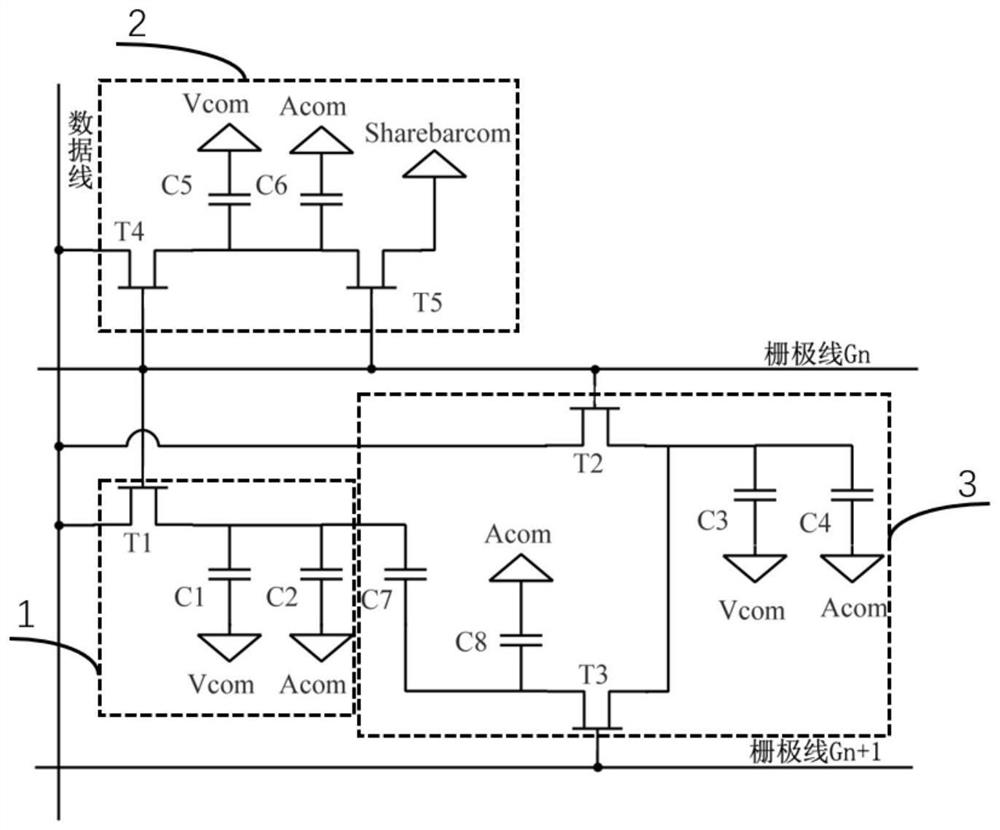
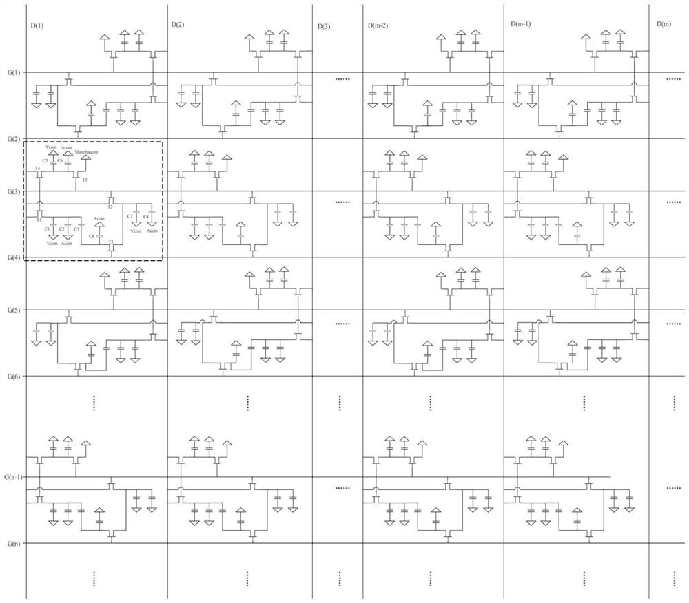
[0027] pixel structure, such as figure 1 As shown, it includes sub-pixel 1 in the main area, sub-pixel 2 in the middle area, and sub-pixel 3 in the sub-area; by controlling the voltage of the three sub-pixels, 12-domain display can be realized, and the large viewing angle deviation of the liquid crystal display panel can be improved. The voltages of the liquid crystal capacitors C1, C3 and C5 of the three sub-pixels are different, so the deflection angles of the liquid crystals are different, which can greatly improve the large viewing angle deviation. The sub-pixel 1 in the main area includes a first thin film transistor T1, a first liquid crystal ca...
PUM
 Abstract
Description
Claims
Application Information

