Transistor forming equipment
A molding equipment and transistor technology, applied in the field of transistors, can solve problems such as pulling deformation
- Summary
- Abstract
- Description
- Claims
- Application Information
AI Technical Summary
Problems solved by technology
Method used
Image
Examples
Embodiment 1
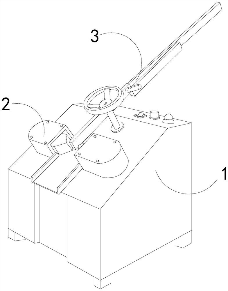
[0026] For example figure 1 -example Figure 5 Shown:
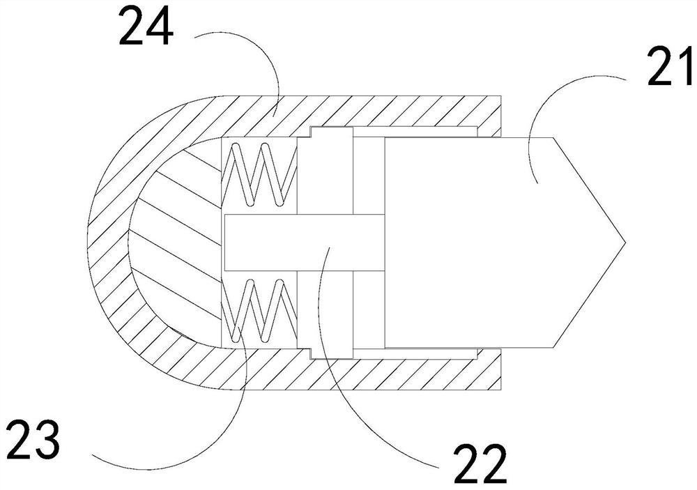
[0027] The present invention provides a transistor forming device, the structure of which includes a body 1, a forming mechanism 2, and a pusher rod 3, the pusher rod 3 is connected to the upper surface of the body 1, and the forming mechanism 2 is embedded in the body 1 The upper end position; the forming mechanism 2 includes a push block 21, a linkage frame 22, a booster bar 23, and an outer frame 24. The push block 21 is embedded in the front end of the linkage frame 22, and the linkage frame 22 and the outer frame 24 The inner side of the pusher bar 23 is installed between the outer frame 24 and the linkage frame 22 .
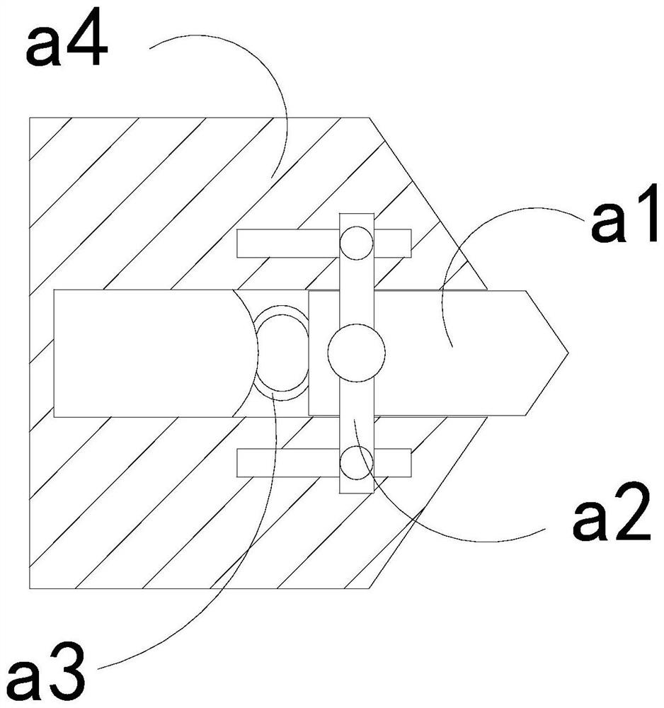
[0028] Wherein, the push block 21 includes a force plate a1, a connecting frame a2, an elastic piece a3, and a plate body a4, the force plate a1 is movably engaged with the plate body a4 through the connecting frame a2, and the elastic piece a3 is installed Between the force plate a1 and the plate b...
Embodiment 2
[0034] For example Image 6 -example Figure 8 Shown:
[0035] Wherein, the plate body a4 includes an outer contact surface c1, a fixed plate c2, a collision plate c3, and a reset piece c4, the left side of the outer contact surface c1 is attached to the right side of the fixed plate c2, and the fixed plate c2 Engaging with the interference plate c3, the reset piece c4 is installed between the fixed plate c2 and the interference plate c3. There are two fixed plates c2, and they are evenly distributed symmetrically on the right side of the interference plate c3. The extrusion produced by the object on the fixed plate c2 can make the fixed plate c2 contract to the left.
[0036] Wherein, the outer contact surface c1 includes a protruding plate c11, an elastic ring c12, and a plate c13. The protruding plate c11 is in clearance fit with the plate c13, and the elastic ring c12 is installed between the inner walls of the protruding plate c11 and the plate c13. Between them, there...
PUM
 Abstract
Description
Claims
Application Information


