Display panel, preparation method thereof and display device

A display panel and display area technology, applied in identification devices, semiconductor/solid-state device manufacturing, instruments, etc., can solve problems such as poor bendability and unfavorable display panel bending, and achieve the effect of improving packaging performance and bending ability

Pending Publication Date: 2021-03-23
HEFEI VISIONOX TECH CO LTD
View PDF6 Cites 2 Cited by
  • Summary
  • Abstract
  • Description
  • Claims
  • Application Information

AI Technical Summary

Problems solved by technology

[0003] In the prior art, thin-film packaging technology is usually used to package OLED devices, but the thin-film packaging structure in the prior art has poor bendability, which is not conducive to the realization of bending of the display panel.

Method used


Image

  • Display panel, preparation method thereof and display device
  • Display panel, preparation method thereof and display device
  • Display panel, preparation method thereof and display device

Examples


Embodiment Construction

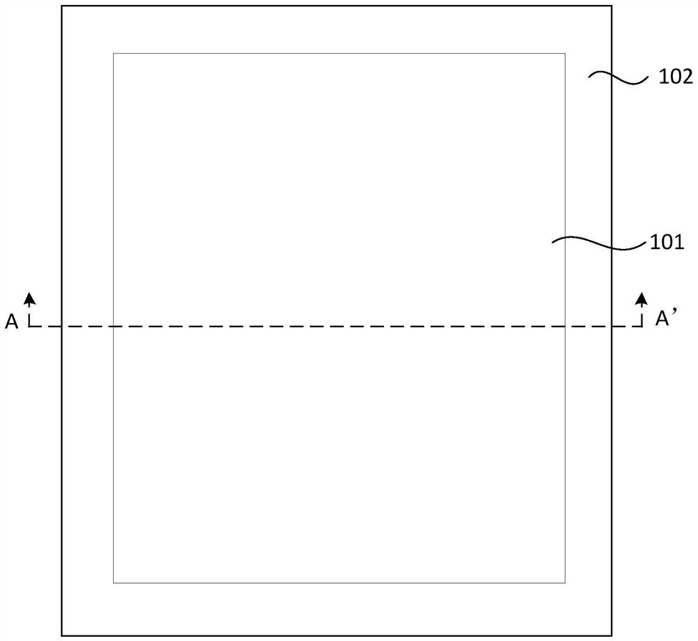
[0034] The present invention will be further described in detail below in conjunction with the accompanying drawings and embodiments. It should be understood that the specific embodiments described here are only used to explain the present invention, but not to limit the present invention. In addition, it should be noted that, for the convenience of description, only some structures related to the present invention are shown in the drawings but not all structures.

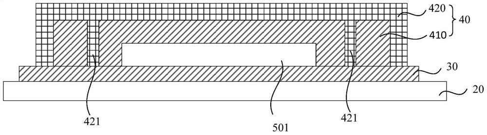
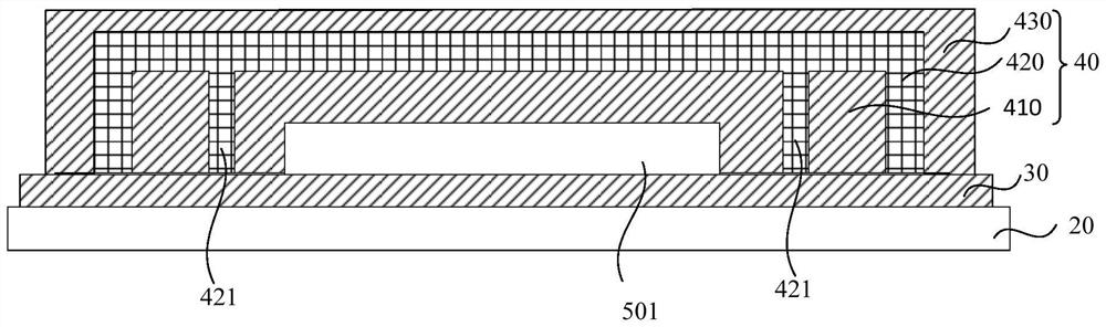
[0035] As mentioned in the background technology, the existing packaging structure usually adopts the method of continuously covering the organic layer and the inorganic layer to package the OLED device. During the bending process of the display panel, there is a large stress between the film layers, and the inorganic layer has Brittleness is easy to break when subjected to a large stress, so that the packaging structure is greatly restricted during the bending process, which is not conducive to the bending of the ...


PUM

PropertyMeasurementUnit
thicknessaaaaaaaaaa
widthaaaaaaaaaa

Abstract

The embodiment of the invention discloses a display panel, a preparation method thereof and a display device. The display panel comprises a substrate, a first water vapor barrier layer, an OLED devicelayer and a second water vapor barrier layer, wherein the second water vapor barrier layer comprises a first inorganic layer and a buffer stress layer which are stacked, the buffer stress layer is located on the side, which is away from the substrate, of the first inorganic layer, the first inorganic layer and the first water vapor barrier layer wrap the OLED device layer, the buffer stress layerand the first water vapor barrier layer wrap the OLED device layer, the buffer stress layer comprises a buffer part, and the buffer part is embedded into the first inorganic layer. According to the technical scheme provided by the embodiment of the invention, the light-emitting unit is wrapped by the first water vapor barrier layer and the second water vapor barrier layer to form a double-layer sealed packaging structure, the packaging effect of the OLED device layer can be improved, and the bending stress of the first inorganic layer can be reduced by embedding the buffer part into the firstinorganic layer, so that the bending capability of the display panel is improved.

Description

technical field [0001] Embodiments of the present invention relate to the field of display technologies, and in particular, to a display panel, a manufacturing method thereof, and a display device. Background technique [0002] The optical materials and electrodes in OLED devices are very sensitive to water vapor and oxygen, and the penetration of water and oxygen will greatly shorten the life of OLED devices. In order to ensure the reliability of display panels, OLED devices have very high requirements for packaging effects. [0003] In the prior art, thin film packaging technology is generally used to package OLED devices, but the thin film packaging structure in the prior art has poor bendability, which is not conducive to realizing bending of the display panel. Contents of the invention [0004] Embodiments of the present invention provide a display panel, a manufacturing method thereof, and a display device, so as to improve the bending ability of the display panel. ...

Claims


Application Information

Patent Timeline
Patent Type & Authority Applications(China)
IPC IPC(8): H01L51/52H01L27/32G09F9/30
CPCG09F9/301H10K59/00H10K50/844H10K50/84
Inventor 莫锦君张明福
Owner HEFEI VISIONOX TECH CO LTD
Why Eureka
Try Eureka