Photosensitive chip assembly, mobile terminal, camera module and preparation method thereof

A photosensitive chip and camera module technology, applied in the field of photography, can solve the problems of blurring around and poor photographing quality, and achieve the effect of reducing field curvature and poor photographing quality.

Active Publication Date: 2021-07-16
NINGBO SUNNY OPOTECH CO LTD
View PDF10 Cites 2 Cited by
  • Summary
  • Abstract
  • Description
  • Claims
  • Application Information

AI Technical Summary

Problems solved by technology

This leads to the camera taking pictures with clear m

Method used


Image

  • Photosensitive chip assembly, mobile terminal, camera module and preparation method thereof
  • Photosensitive chip assembly, mobile terminal, camera module and preparation method thereof
  • Photosensitive chip assembly, mobile terminal, camera module and preparation method thereof

Examples


Embodiment Construction

[0095] The specific implementation manners of the present invention will be described in more detail below with reference to the drawings and embodiments, so as to better understand the solutions of the present invention and the advantages of various aspects. However, the specific embodiments and examples described below are for the purpose of illustration only, rather than limiting the present invention.

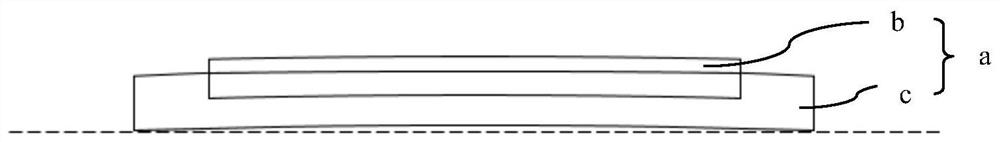
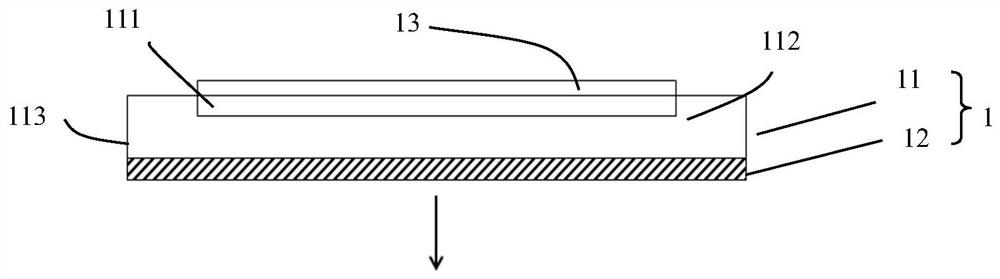
[0096] figure 1 It is a schematic diagram of the deformation state of a traditional photosensitive chip. figure 2 It is a schematic structural diagram of a photosensitive chip assembly according to an embodiment of the present application. Figure 3a It is a schematic diagram of a deformed photosensitive chip according to an embodiment of the present application. Figure 3b It is a schematic diagram of the protruding distance of the part in the photosensitive chip to the direction of the stress film in an embodiment of the present application. Figure 4a It is a schemat...


PUM

PropertyMeasurementUnit
Thicknessaaaaaaaaaa
Thicknessaaaaaaaaaa
Areaaaaaaaaaaa

Abstract

The invention discloses a photosensitive chip assembly, and a camera module and a mobile terminal using the photosensitive chip assembly. The photosensitive chip assembly comprises a photosensitive chip which is provided with a photosensitive area and a non-photosensitive area located at the edge of the photosensitive area, wherein the photosensitive area receives light reaching the front face of the photosensitive chip; a stress film which is attached to the back face of the photosensitive chip and has a preset thickness, wherein the stress generated in the stress film enables the photosensitive area of the photosensitive chip to deform towards the back face of the photosensitive chip. According to the photosensitive chip disclosed by the invention, the stress film is plated on the back surface of the photosensitive chip, and the stress generated by the stress film enables the photosensitive chip to deform towards the back surface of the photosensitive chip, so that the condition that the central area or the photosensitive area of the photosensitive chip protrudes towards the front surface of the photosensitive chip after the heating and curing process of the camera module is counteracted or reduced; and the phenomenon of poor photographing quality caused by field curvature is reduced. The invention also utilizes the photosensitive chip assembly to manufacture a camera module.

Description

technical field [0001] The present application mainly relates to the field of imaging, and in particular to a photosensitive chip assembly, a camera module and a mobile terminal using the photosensitive chip assembly. Background technique [0002] Cameras are essential input devices in electronic products such as mobile phones and tablet computers. As users continue to improve the image quality of cameras, the pixels of cameras are also getting larger. [0003] The process of camera imaging is mainly the process of digitizing optical signals, which is mainly completed by the camera module. The camera module mainly includes a lens, a photosensitive chip and a circuit board. The photosensitive chip is the main component of the camera module. Its working principle is: the external light passes through the lens and shines on the surface of the photosensitive chip, and the photosensitive chip transmits the light transmitted by the lens. It is converted into an electrical signal...

Claims


Application Information

Patent Timeline
IPC IPC(8): H04N5/225
CPCH04N23/54H04N23/55
Inventor 蒋恒孟楠
Owner NINGBO SUNNY OPOTECH CO LTD
Why Eureka
Try Eureka