Display panel

A display panel and substrate technology, applied in identification devices, instruments, etc., can solve the problems of display panel cost increase, small line width design accuracy doubts, circuit overheating, etc., to reduce production costs and circuit overheating risks, and reduce line width accuracy Requirements, the effect of reducing the production cost

Active Publication Date: 2021-08-20
AU OPTRONICS CORP
View PDF11 Cites 0 Cited by
  • Summary
  • Abstract
  • Description
  • Claims
  • Application Information

AI Technical Summary

Problems solved by technology

However, today’s vertical gate technology must use double-layer chip-on-chip films, which leads to a substantial increase in the cost of the display panel. In addition, the fine line

Method used


Image

  • Display panel
  • Display panel
  • Display panel

Examples


Embodiment Construction

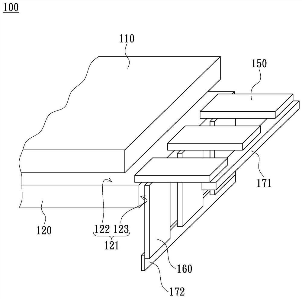
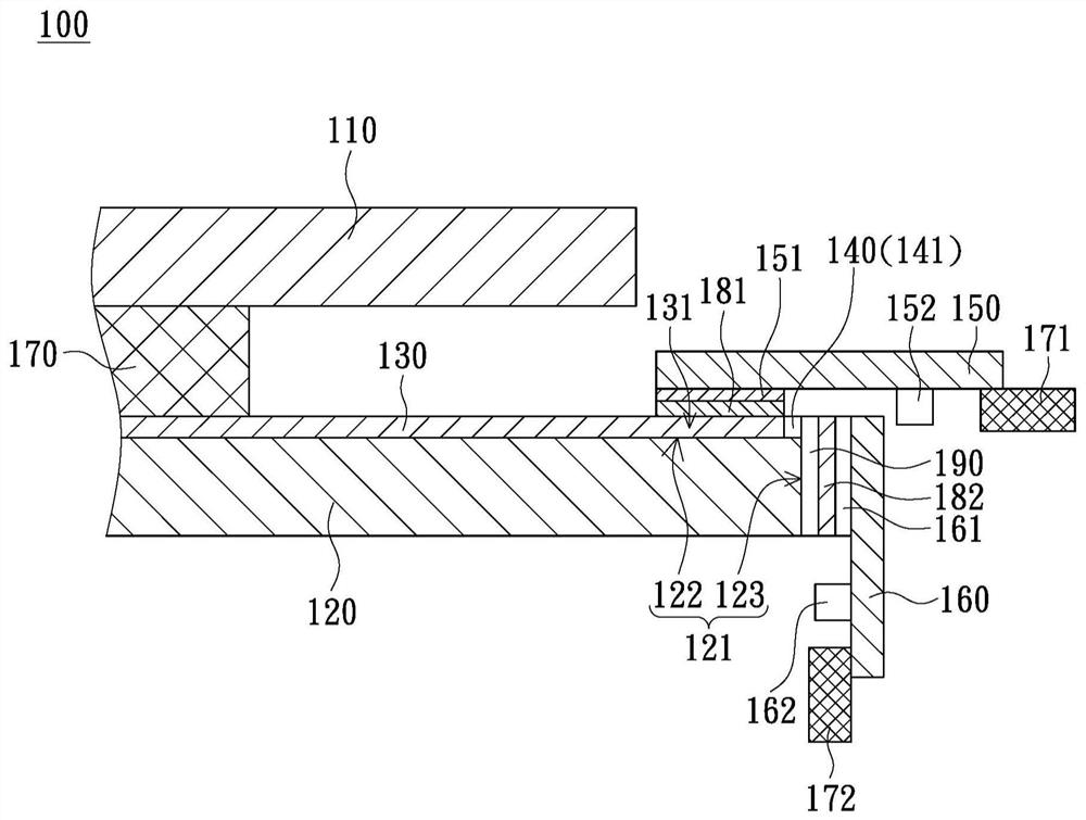
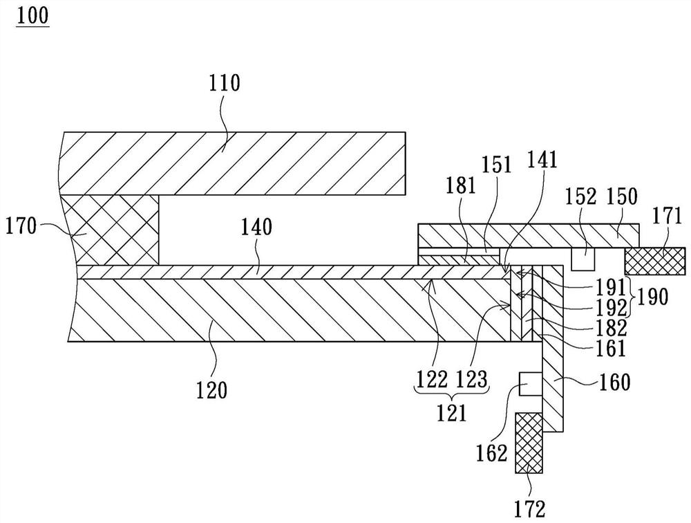
[0052] figure 1 It is a partial perspective view of a display panel according to an embodiment of the present invention. figure 2 for figure 1 A schematic cross-sectional view of the display panel shown. image 3 for figure 1 Another schematic cross-sectional view of the display panel shown. Figure 4 for figure 1 A schematic right-side view of the display panel shown. Figure 5 for figure 1 A schematic top view of the display panel shown. For easy understanding, the Figure 4 Omit the first circuit board 150, the third bonding end 151, the first driver chip 152, the second circuit board 160, the second driver chip 162, the first external circuit board 171, the second external circuit board 172 and the upper conductive bonding layer 181 , and at Figure 5 Omit the first circuit board 150, the third bonding end 151, the first driving chip 152, the second circuit board 160, the fourth bonding end 161, the second driving chip 162, the first external circuit board 171, a...


PUM


Abstract

A display panel can reduce cost, overheating risk and line width precision requirements, and comprises: a first substrate; a second substrate, which is arranged below the first substrate and is provided with a joint end part, and the joint end part is provided with an upper surface and a side surface which are connected with each other; a plurality of first circuits, which are arranged on the second substrate at intervals, wherein each first circuit is provided with a first joint end arranged on the upper surface; a plurality of second circuits, which are arranged on the second substrate at intervals and are separated from the first circuits, wherein each second circuit is provided with a second joint end arranged at the joint of the side surface and the upper surface; a first circuit board, which is located on the upper surface and provided with a plurality of third joint ends, wherein the third joint ends are electrically connected with the first joint ends respectively; and a second circuit board, which is positioned on the side surface and is provided with a plurality of fourth joint ends, wherein the fourth joint ends are electrically connected with the second joint ends respectively.

Description

technical field [0001] The invention relates to a display panel. Background technique [0002] The vertical gate (Vertical-gate) technology that the display panel has developed so far pulls the data (data) line and the gate (gate) line to one side of the display panel, and uses a double-layer chip on film (2-layered chip on film) ), the source driver chip and the gate driver chip are made on the double-layer chip-on-chip film, so that the border on the non-outer lead bonding side can be less than 1 mm, in order to achieve Need for ultra-narrow bezels. However, today’s vertical gate technology must use double-layer chip-on-chip films, resulting in a significant increase in the cost of the display panel, and the fine line width design required by this vertical gate technology also has doubts about the accuracy, and it will also be used for a long time. Problems that cause circuits to overheat. Contents of the invention [0003] The present invention provides a display pan...

Claims


Application Information

Patent Timeline
IPC IPC(8): G09F9/30
CPCG09F9/30
Inventor 颜子贤徐雅玲黄朝伟林雅慧杨人中
Owner AU OPTRONICS CORP
Why Eureka
Try Eureka