Thick film circuit hole metallization method and thick film circuit printing method

A thick-film circuit and hole metallization technology, which is applied in the manufacture of circuits, electrical components, semiconductors/solid-state devices, etc., can solve the problems of low qualified rate of through-hole connection, uneven distribution of conductive paste, and high price

Pending Publication Date: 2021-09-10
CHUANYI MICROCIRCUIT CHONGQING
View PDF9 Cites 1 Cited by
  • Summary
  • Abstract
  • Description
  • Claims
  • Application Information

AI Technical Summary

Problems solved by technology

The current common through-hole printing process technology 1: the substrate is placed on the negative pressure cavity, and the slurry is pulled to flow down along the wall of the through hole of the substrate by negative pressure, and the operation is repeated on both sides to form a double-sided connection; however, the negative pressure cavity The suction force is unbalanced, the conductive paste on the inner wall of each through hole is unevenly distributed, and the conductive paste on the inner wall of the through hole with a smaller aperture is easy to overflow and affect the other side, making the connection pass rate of the through hole low
Through-hole printing technology 2: Use special hole-filling paste to fill the through-holes during printing; however, special paste with high price is required, and the number of printings is high, and the temperature expansion coefficient of the hole-filling paste cannot completely match the substrate, resulting in products There is a certain temperature limit for use

Method used


Image

  • Thick film circuit hole metallization method and thick film circuit printing method
  • Thick film circuit hole metallization method and thick film circuit printing method
  • Thick film circuit hole metallization method and thick film circuit printing method

Examples


Embodiment Construction

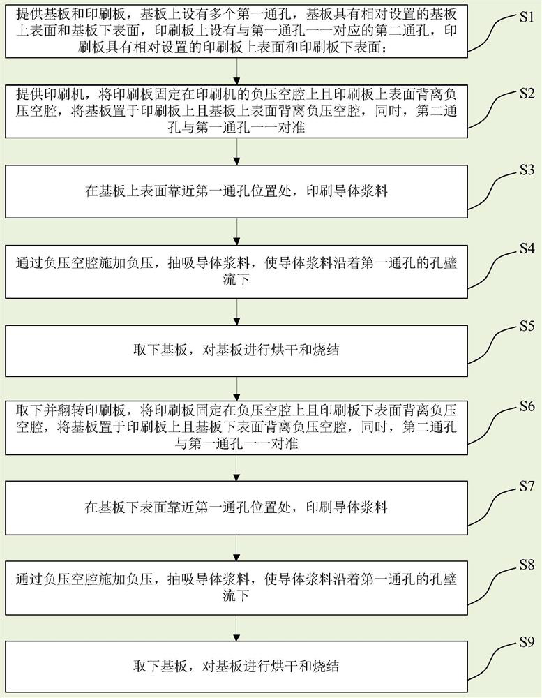
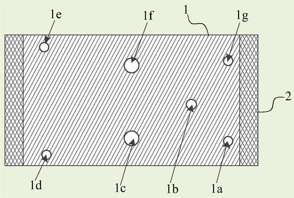
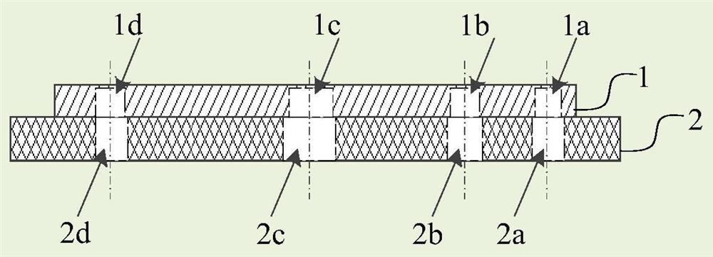
[0041] As mentioned above in the background technology, at present, the common process of hole metallization (double-sided conduction) of thick-film circuits is realized by through-hole printing, drying, and sintering of conductive paste. There are mainly the following two The first method: the substrate is placed on the negative pressure cavity, and the slurry is pulled by negative pressure to flow down the hole wall of the through hole of the substrate, and the operation is repeated on both sides to form a double-sided connection. However, the suction force of the negative pressure cavity is not balanced, The conductive paste on the inner wall of each through-hole is unevenly distributed, and the conductive paste on the inner wall of the through-hole with a smaller aperture is easy to overflow and affect the other side, making the connection pass rate of the through-hole low; using special hole-filling paste, it is filled during printing Through-holes, however, require high-p...


PUM


Abstract

The invention provides a thick film circuit hole metallization method and a thick film circuit printing method. The suction pressure of a negative pressure cavity on first through holes with various sizes on a substrate is buffered and balanced through a printing plate which is arranged between the negative pressure cavity and the substrate and is provided with second through holes, so that the negative pressure in the negative pressure cavity can be uniformly transmitted to the first through hole in the substrate along the second through holes in the printing plate, further a conductor paste near the first through hole can uniformly flow down along the hole wall of the first through hole, and the connection qualification rate of the double-sided circuit of the substrate is improved; and the suction pressure of the negative pressure cavity is relieved, the problem that the substrate is polluted due to the fact that the conductor slurry overflows to the other side of the substrate from the first through hole can be avoided, and the product percent of pass and quality are further improved while conventional conductor slurry which is not limited by temperature can be utilized to perform hole metallization, so that the cost is reduced.

Description

technical field [0001] The invention relates to the technical field of thick-film circuit manufacturing, in particular to a thick-film circuit hole metallization method and a thick-film circuit printing method. Background technique [0002] At present, thick-film circuits are widely used in industrial electronic products. The design of thick-film circuits is inseparable from the wiring design of circuits. With the improvement of the integration requirements of thick-film integrated circuits, double-sided printed wiring technology has emerged. Among them , the circuit wires on the two sides are connected and conducted to enable the thick film circuit to perform its basic functions, which requires the use of external wires or through holes. [0003] Among them, the double-sided conduction of thick film circuits is usually realized by through-hole printing, drying, and sintering of conductive paste. The current common through-hole printing process technology 1: the substrate i...

Claims


Application Information

Patent Timeline
Patent Type & Authority Applications(China)
IPC IPC(8): H01L21/48H01L21/70H01L21/67
CPCH01L21/486H01L21/4867H01L21/705H01L21/67253
Inventor 李林军谭朗
Owner CHUANYI MICROCIRCUIT CHONGQING
Why Eureka
Try Eureka